Multi-conducting through hole structure

a multi-conducting, through hole technology, applied in the direction of printed circuit manufacturing, printed circuit aspects, basic electric elements, etc., can solve the problem of limiting the layout density of the circuit board, conventional pth forms a limitation, etc., to promote signal-transmission quality and lower cross-talk problems

Active Publication Date: 2008-12-30
VIA TECH INC
View PDF10 Cites 15 Cited by
  • Summary
  • Abstract
  • Description
  • Claims
  • Application Information

AI Technical Summary

Benefits of technology

[0011]An object of the present invention is to provide a multi-conducting through hole structure capable of reducing electromagnetic coupling between signals and lowering the cross-talk therefrom.
[0015]In the present invention, because the reference line is disposed between the signal lines, the signal interference between the signal lines is shielded by the reference line. Therefore, the alternate capacitance and inductance derived from the electromagnetic coupling between the signals will be reduced so as to lower the cross-talk problem and to promote the signal-transmission quality.

Problems solved by technology

Since the conventional PTH occupies a larger area on a circuit board, the conventional PTH forms a limitation for raising the layout density of the circuit board.

Method used


Image

  • Multi-conducting through hole structure
  • Multi-conducting through hole structure
  • Multi-conducting through hole structure

Examples


Embodiment Construction

[0024]Various specific embodiments of the present invention are disclosed below, illustrating examples of various possible implementations of the concepts of the present invention. The following description is made for the purpose of illustrating the general principles of the invention and should not be taken in a limiting sense. The scope of the invention is best determined by reference to the appended claims.

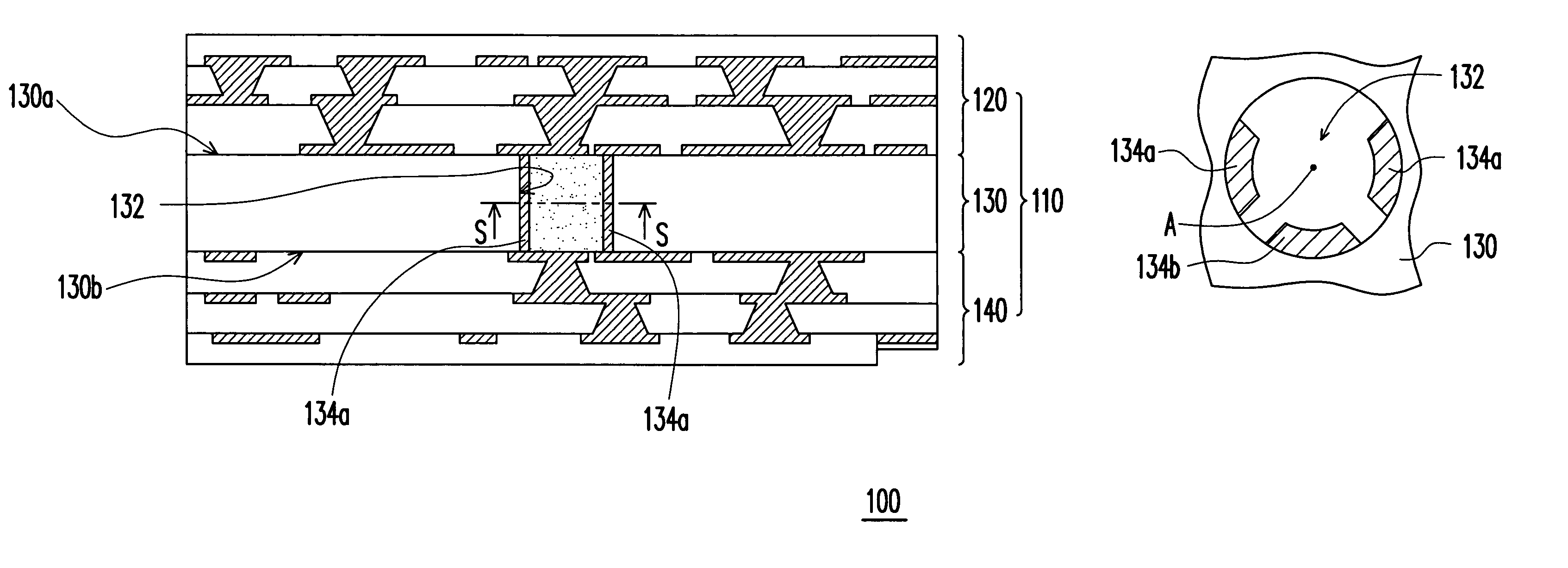
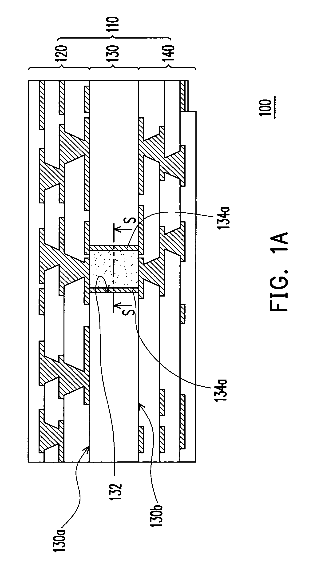
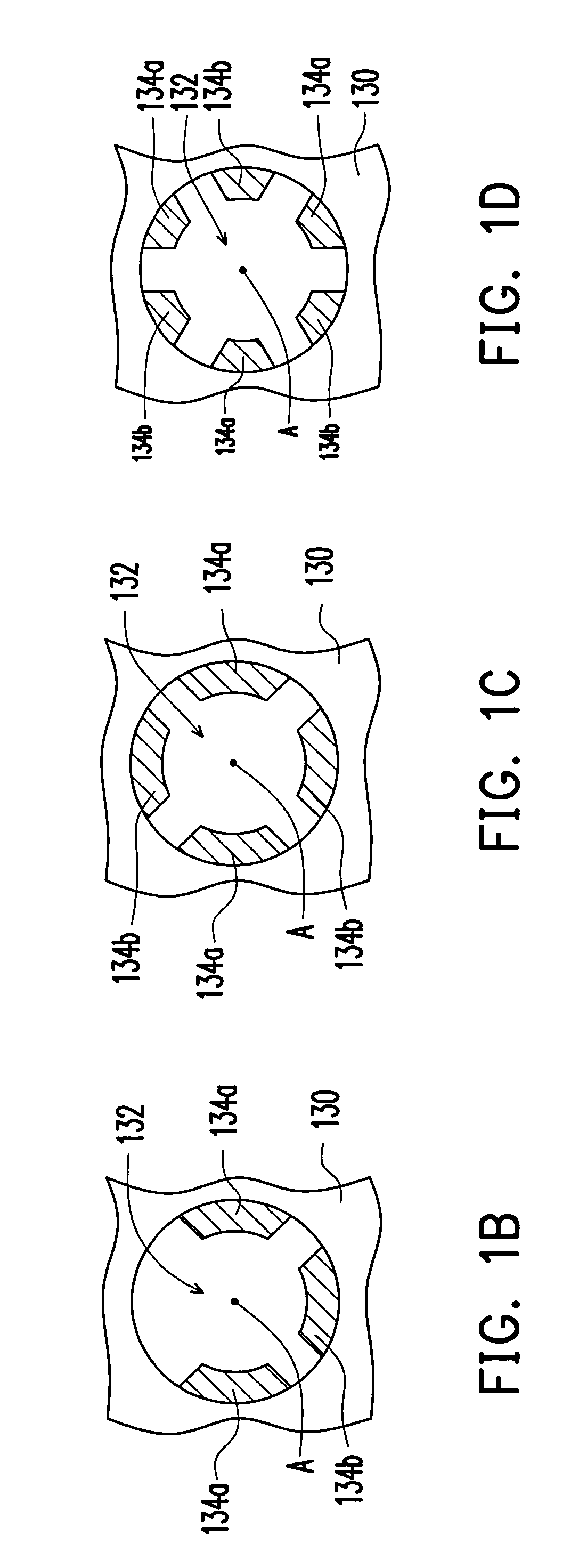
[0025]FIG. 1A is a vertical cross-sectional view of a multi-conducting through hole structure according to one embodiment of the present invention. FIG. 1B is a horizontal cross-sectional view taken along line S-S in FIG. 1A. Referring to FIG. 1A and FIG. 1B, a circuit board 100, having altogether patterned circuit layers and dielectric layers is used as an example in FIG. 1A. The circuit board 100 has a multi-layer circuit structure 110 comprising a top circuit structure 120, a dielectric core layer 130 and a bottom circuit structure 140. The top circuit structure 120 compris...


PUM


Abstract

A multi-conducting through hole structure is provided. The multi-conducting through hole structure has a substrate, at least two signal lines and at least a reference line. The substrate has a through hole passing therethrough. The signal lines are disposed on a portion of an inner surface of the through hole and extended through the through hole. The reference line is disposed on a portion of the inner surface of the through hole and extended through the through hole, wherein the reference line is disposed between the lines for signal. Because the signal lines are separated by the reference line, the electromagnetic coupling generated by signals can be reduced to lower the cross-talk interference between signals passing through the through hole, so as to promote the signal-transmission quality.

Description

CROSS-REFERENCE TO RELATED APPLICATION[0001]This application is a continuation-in-part of a prior application Ser. No. 11 / 065,496, filed Feb. 23, 2005, which claims the priority benefit of Taiwan application serial no. 93105346, filed on Mar. 2, 2004. All disclosures are incorporated herewith by reference.BACKGROUND OF THE INVENTION[0002]1. Field of the Invention[0003]The present invention generally relates to a signal transmission structure, in particular, the present invention relates to a multi-conducting through hole structure which can be used in a circuit board.[0004]2. Description of Related Art[0005]A conventional circuit board comprises multiple patterned circuit layers and a plurality of dielectric layers alternately laminated on top of each other. The patterned circuit layers are formed, for example, by patterning copper foils in a photolithographic process and an etching process. The dielectric layers are disposed between two neighboring patterned circuit layers to isola...

Claims


Application Information

Patent Timeline
Patent Type & Authority Patents(United States)
IPC IPC(8): H05K1/11
CPCH05K1/0222H05K3/4602H05K1/115H05K3/0035H05K2201/09645
Inventor HO, KWUN-YAOKUNG, MORISSHSU, CHI-HSINGHSU, JIMMY
Owner VIA TECH INC
Why Eureka
Try Eureka