Wide bandgap semiconductor double-sided heat dissipation module packaging structure based on conductive metal band

A wide-bandgap semiconductor and conductive metal strip technology, applied in semiconductor devices, semiconductor/solid-state device components, and electrical solid-state devices, etc., can solve the problems of bond point connection failure, harsh heat dissipation environment, and large chip thermal resistance. Enhance current flow capacity, improve space utilization, reduce the effect of common source inductance

Pending Publication Date: 2022-06-21
XI AN JIAOTONG UNIV
View PDF0 Cites 2 Cited by
  • Summary
  • Abstract
  • Description
  • Claims
  • Application Information

AI Technical Summary

Problems solved by technology

[0005] 2. The thermal performance of traditional power modules is difficult to meet the requirements of wide bandgap semiconductor power chips
The heat dissipation of traditional power modules adopts a single-sided heat dissipation method. The heat dissipation of semiconductor power chips mainly relies on a single heat dissipation path through the bottom substrate and heat sink. The thermal resistance from the chip to the surrounding environment is large, which is very unfavorable for the long-term reliable operation of the power module; At the same time, most traditional power modules use aluminum bonding wires for electrical interconnection. When the heat cannot be dissipated well, connection failures are prone to occur at the bonding points. Although the thermal conductivity of silicon carbide is higher than that of silicon, the chip area is much smaller than that of silicon. , the heat dissipation environment is more severe
The selection of traditional module packaging materials matches the thermal expansion coefficient of silicon. However, the thermal expansion coefficient of wide-bandgap semiconductor materials is quite different from that of silicon, which is prone to thermal reliability problems.
[0006] 3. It is difficult for traditional power modules to achieve current sharing of power chips, and this performance is crucial at high switching frequencies
The difference in parasitic inductance will cause the dynamic current distribution of the chip to be uneven, and the temperature difference and thermal coupling of the chip will cause the static current distribution of the chip to be uneven.
Especially since the switching speed of the wide bandgap power semiconductor chip is much higher than that of silicon, in the dynamic switching process, it is more likely to cause chip breakdown and temperature difference expansion, thereby further accelerating the overall failure process of the module
[0007] To sum up, power chips based on wide-bandgap semiconductor materials are limited by traditional packaging, and do not exert the excellent electrical and thermal properties that the material itself should have.

Method used


Image

  • Wide bandgap semiconductor double-sided heat dissipation module packaging structure based on conductive metal band
  • Wide bandgap semiconductor double-sided heat dissipation module packaging structure based on conductive metal band
  • Wide bandgap semiconductor double-sided heat dissipation module packaging structure based on conductive metal band

Examples


Embodiment

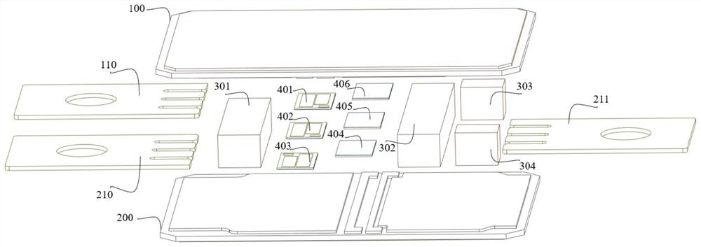
[0067] see figure 1 , figure 2 , image 3 and Figure 4 , the package structure of this embodiment includes 2 power substrates, 2 groups of 6 wide bandgap power semiconductor chips, 4 power pads, 3 power terminals, 8 drive terminals and 6 groups of conductive metal strips.

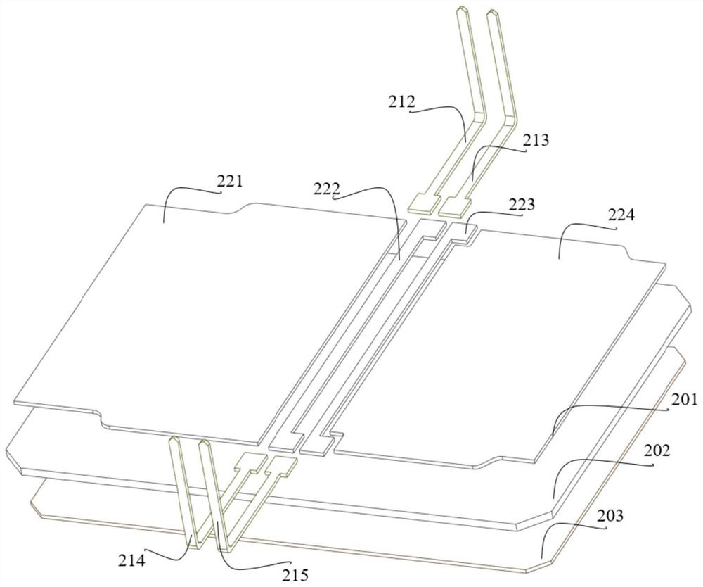
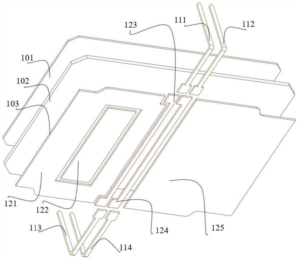
[0068] The two power substrates are specifically the top power substrate 100 and the bottom power substrate 200 .

[0069] The six wide-bandgap power semiconductor chips 400 are specifically a first high-arm wide-bandgap power semiconductor chip 401, a second high-arm wide-bandgap power semiconductor chip 402, a third high-arm wide-bandgap power semiconductor chip 403, The first lower arm wide bandgap power semiconductor chip 404 , the second lower arm wide bandgap power semiconductor chip 405 and the third lower arm wide bandgap power semiconductor chip 406 .

[0070] The four power pads are specifically a DC side power pad 301 , an AC side main power pad 302 , an AC side auxiliary power pad 303 and ...


PUM


Abstract

The invention discloses a wide bandgap semiconductor double-sided heat dissipation module packaging structure based on a conductive metal band, semiconductor power chips of different bridge arms are arranged on different power substrates, the size of a module is reduced, and the power density of the module is greatly improved; the power gasket is arranged between the top power substrate and the bottom power substrate, plays a role in mechanical support and electrical connection, provides an additional heat dissipation path for each semiconductor power chip on the basis of double-sided heat dissipation, reduces the thermal coupling degree between the chips, achieves the chip temperature equalization effect, and improves the heat dissipation environment of the chips; the driving loop and the commutation loop are nearly vertical in space, the electromagnetic coupling degree between the loops is greatly reduced, and the reliability of the module is further improved; the commutation loop uses the conductive metal belt to complete electrical connection required by the chip, the parasitic inductance value of the module is greatly reduced, and the source electrode conductive metal belt is provided with a hole groove at the joint, so that the distribution uniformity of the parasitic inductance can be improved, and the current sharing effect of the chip is achieved.

Description

technical field [0001] The invention belongs to the technical field of semiconductor packaging, and in particular relates to a wide-bandgap semiconductor double-sided heat dissipation module packaging structure based on conductive metal strips. Background technique [0002] A power module is a module formed by repackaging several power semiconductor chips according to a certain functional combination. Compared with discrete power devices, power modules have a high degree of integration, so they have great advantages in electrical performance, thermal performance and economic considerations. [0003] In recent years, with the rapid development of industries represented by new energy grid connection, high-voltage direct current transmission, electric vehicles, high-speed rail, aerospace, and pulse power, the performance requirements of power electronic systems for semiconductor power modules are increasing, which promotes the continuous improvement of power modules. It is dev...

Claims


Application Information

Patent Timeline
Patent Type & Authority Applications(China)
IPC IPC(8): H01L23/367H01L23/49H01L23/16
CPCH01L23/3677H01L23/49H01L23/16H01L2224/0603
Inventor 王来利熊帅张彤宇
Owner XI AN JIAOTONG UNIV
Why Eureka
Try Eureka