Robust MEMS actuator for relays

a relay and actuator technology, applied in the field of microelectromechanical system devices, can solve the problems of unsatisfactory silicon electrical properties,

Inactive Publication Date: 2008-12-30
LUCENT TECH INC
View PDF2 Cites 18 Cited by
  • Summary
  • Abstract
  • Description
  • Claims
  • Application Information

AI Technical Summary

Benefits of technology

[0003]One embodiment of the present disclosure is an apparatus comprising a microelectromechanical system (MEMS) device. The MEMS device includes a substrate having an anchoring pad thereon and a structural element. The structural element has a beam that includes a first part and a second part. The first part is attached to both the anchoring pad and to the second part. The second part is movable with respect to the substrate and is made of an electrically conductive material. Additionally, at least one of the fo...

Problems solved by technology

The electrical properties of silicon, however, are not ideal in applications where components...

Method used


Image

  • Robust MEMS actuator for relays
  • Robust MEMS actuator for relays
  • Robust MEMS actuator for relays

Examples


Embodiment Construction

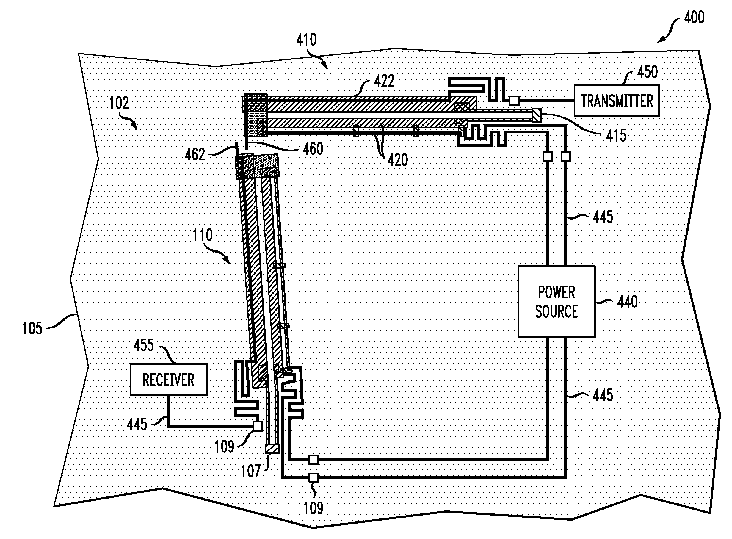
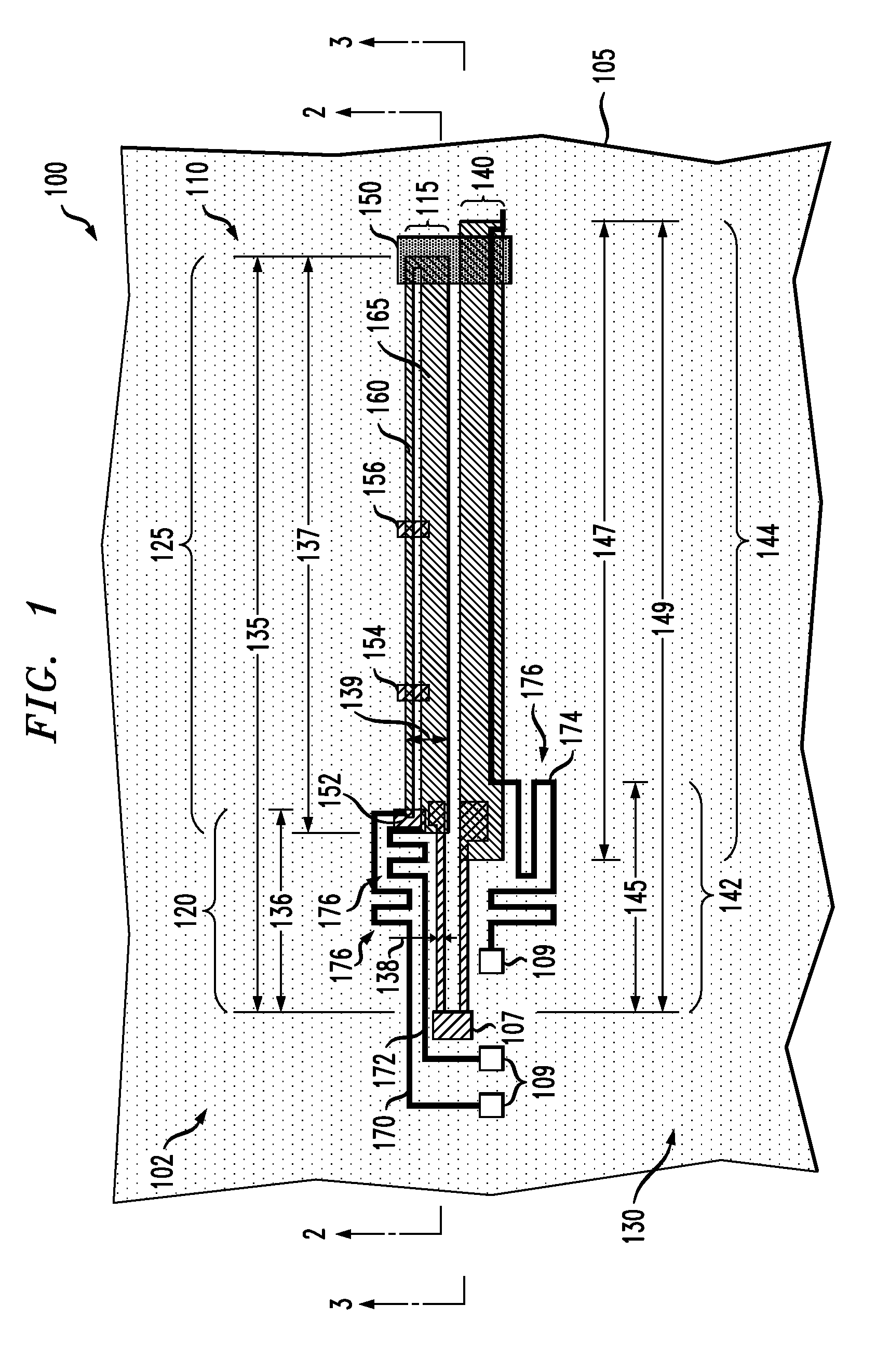
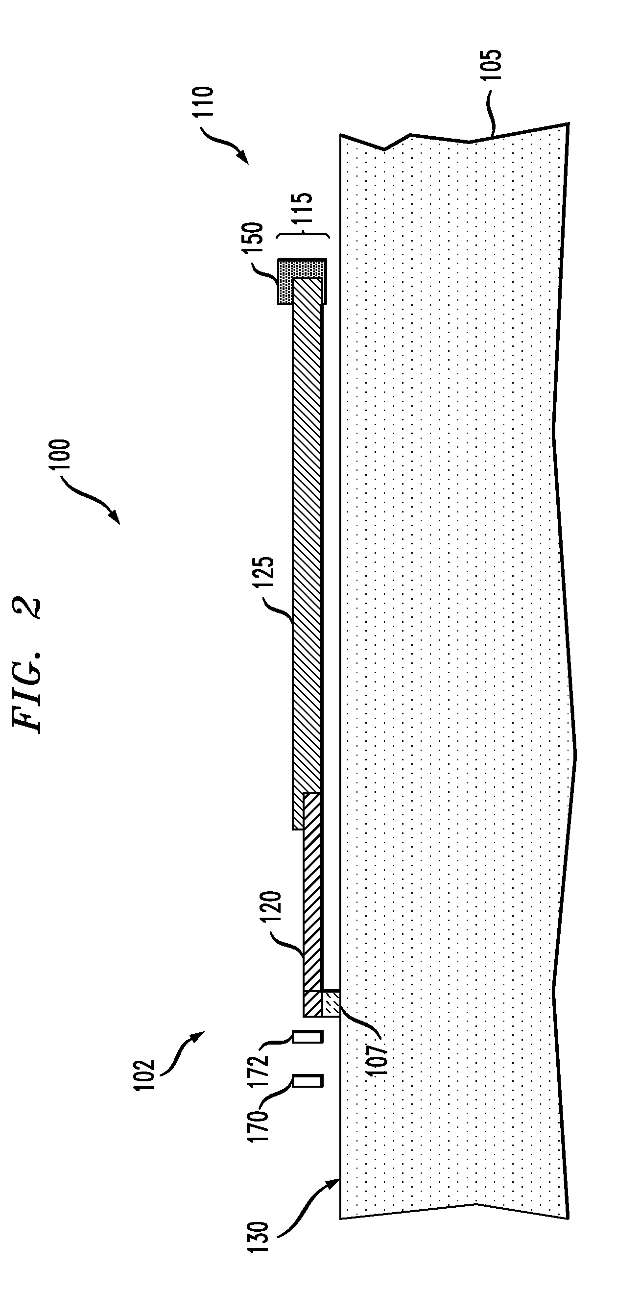
[0013]As part of the present disclosure, it was found that metals used as components in MEMS devices are prone to a number of structural failures. In particular, movable metal components can suffer from plastic deformation, creep deformation and / or fatigue earlier than desired. Yield stress is the stress value at which a material begins to plastically deform. Fatigue is characterized by the number repetitive motions a component can have before it is deformed. Creep relates to a time-dependent plastic deformation activated by stress and / or temperature. Creep is a permanent deformation in a material after a period under a stress that is lower than the yield stress of the material. This stress can occur while the MEMS device is actuated or when latched in a stressed configuration for an extended time. The term creep rate refers to a rate of change in a dimension of a material (e.g., the absolute or percentage change in the length of a long axis of a beam of the device) versus time unde...


PUM


Abstract

An apparatus comprising a microelectromechanical system (MEMS) device. The MEMS device includes a substrate having an anchoring pad thereon and a structural element. The structural element has a beam that includes a first part and a second part. The first part is attached to both the anchoring pad and to the second part. The second part is movable with respect to the substrate and made of an electrically conductive material. Additionally, at least one of the following conditions hold: the first part is made of a material having: a first yield stress that is greater than a second yield stress of the electrically conductive material of the second part; a fatigue resistance that is greater than a second fatigue resistance of the electrically conductive material of the second part; or, a creep rate that is less than a second creep rate of the electrically conductive material of the second part.

Description

TECHNICAL FIELD OF THE INVENTION[0001]The present invention relates, in general, to microelectromechanical system devices, as well as methods of using and manufacturing such devices.BACKGROUND OF THE INVENTION[0002]Silicon (e.g., polysilicon) is one of the most widely-used structural materials for microelectromechanical system (MEMS) devices. The electrical properties of silicon, however, are not ideal in applications where components having a low electrical resistivity and a high coefficient of thermal expansion (CTE) are desired. Metals have been considered as a replacement material for silicon in such applications.SUMMARY OF THE INVENTION[0003]One embodiment of the present disclosure is an apparatus comprising a microelectromechanical system (MEMS) device. The MEMS device includes a substrate having an anchoring pad thereon and a structural element. The structural element has a beam that includes a first part and a second part. The first part is attached to both the anchoring pad...

Claims


Application Information

Patent Timeline
IPC IPC(8): H01H61/01H01L21/00H01L23/58H01L31/04
CPCB81B3/0072H01H61/04B81B2201/032H01H2061/006H01H2061/008
Inventor AKSYUK, VLADIMIR ANATOLYEVICHPARDO, FLAVIOSIMON, MARIA ELINA
Owner LUCENT TECH INC
Why Eureka
Try Eureka