
Substrate processing method

a substrate and processing method technology, applied in the direction of semiconductor/solid-state device testing/measurement, measurement devices, instruments, etc., can solve the problems of significant increase in pattern defects, increase in device pattern defects, etc., to suppress the worsening of the uniformity of the substrate process over the substrate, and reduce the loss of semiconductor device production yield

Active Publication Date: 2009-01-13
PANASONIC SEMICON SOLUTIONS CO LTD
View PDF4 Cites 0 Cited by
  • Summary
  • Abstract
  • Description
  • Claims
  • Application Information

AI Technical Summary

Benefits of technology

This approach effectively suppresses pattern defects and maintains process uniformity, enhancing the reliability and yield of semiconductor devices by controlling the substrate moving velocity within specific limits.

Problems solved by technology

However, as the pattern dimensions of semiconductor elements formed at a semiconductor integrated circuit device are becoming finer, pattern defects of a device into which an impurity is introduced using the ion implantation apparatus of FIG. 4A are increasing.
Furthermore, it has been found that such pattern defects significantly increase, in particular, when the pattern dimensions are set at 130 nm or less.

Method used


Image

  • Substrate processing method
  • Substrate processing method
  • Substrate processing method

Examples


Embodiment Construction

[0058]A substrate processing method of an embodiment of the present invention will be described hereinafter with reference to the drawings.

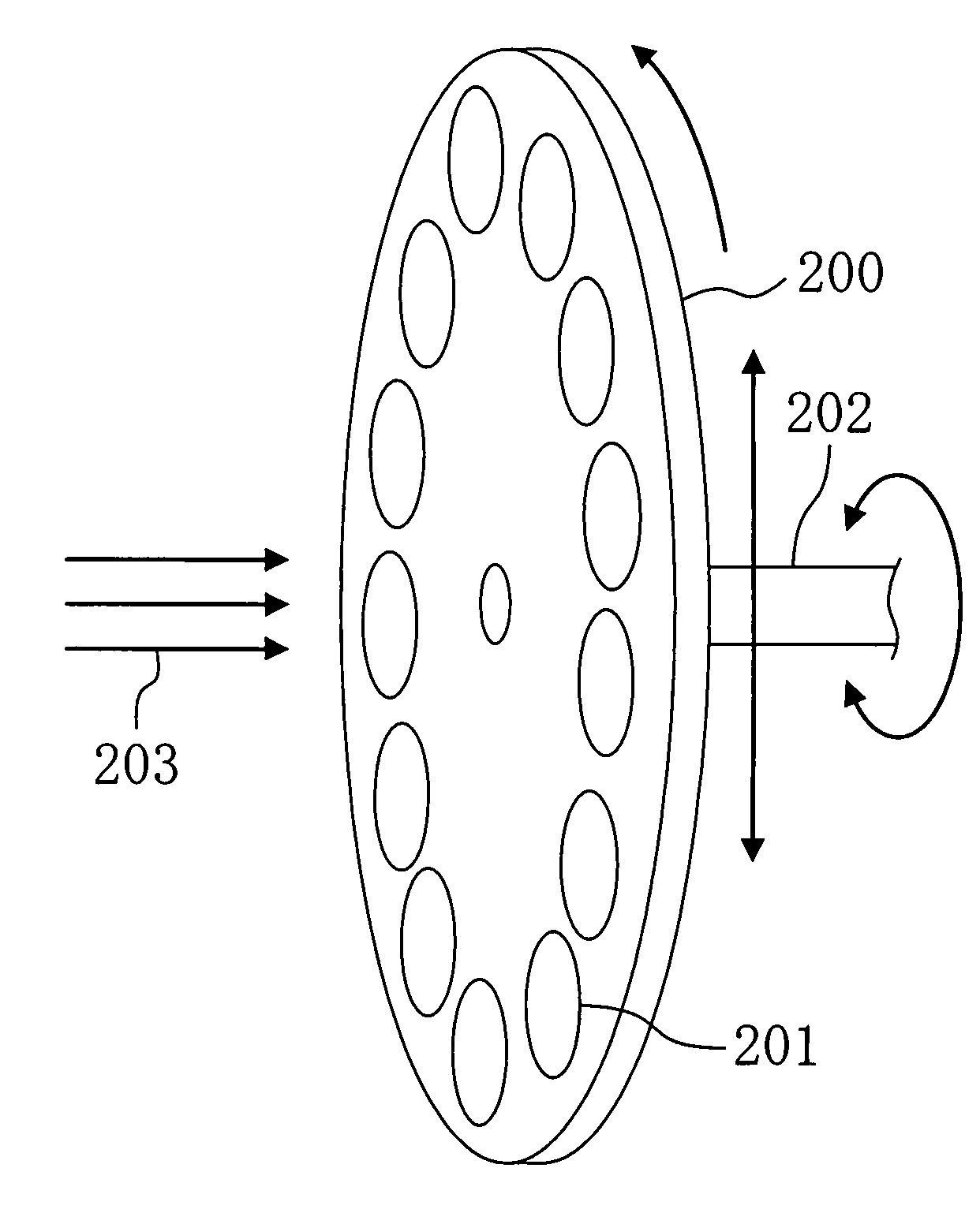
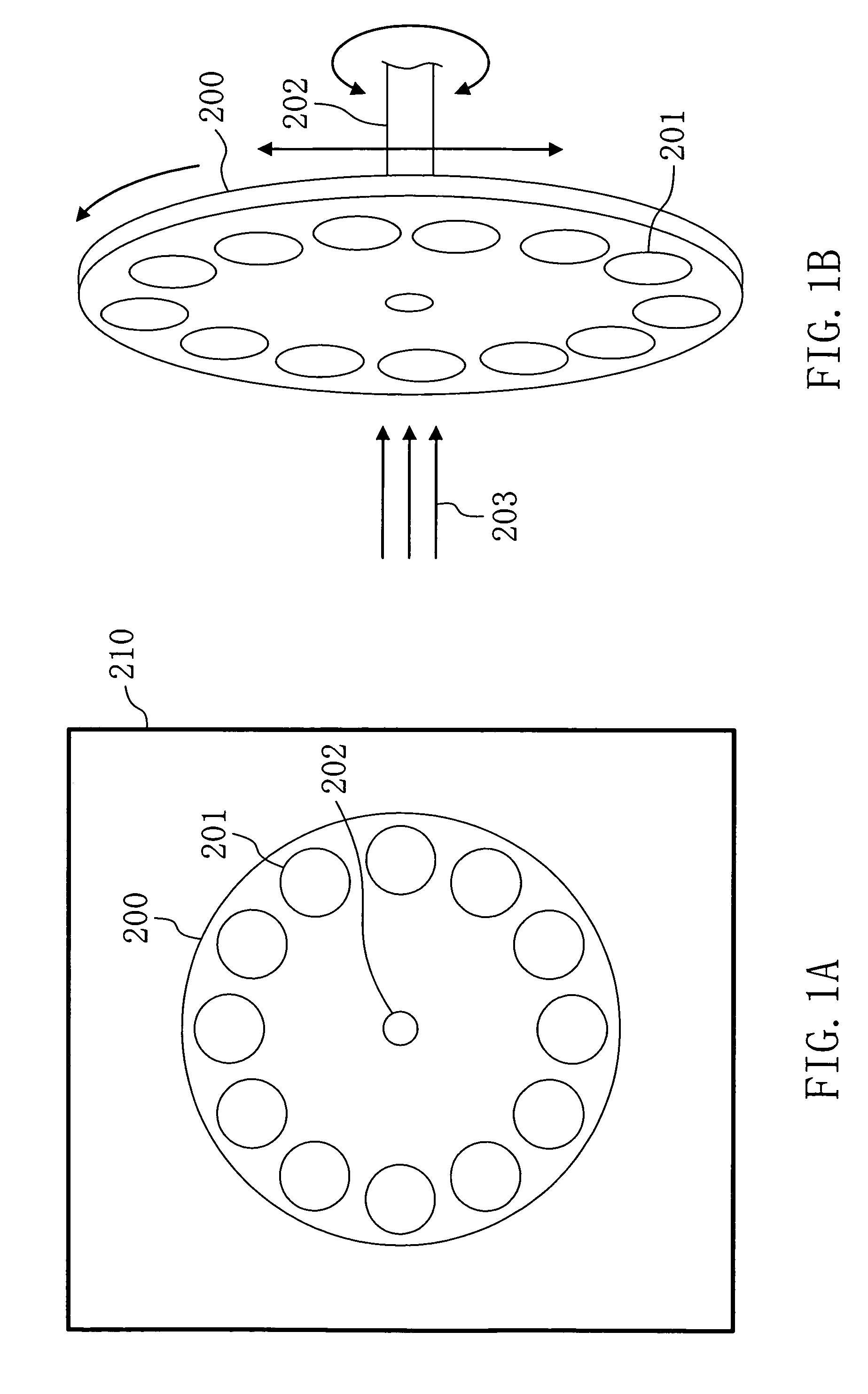
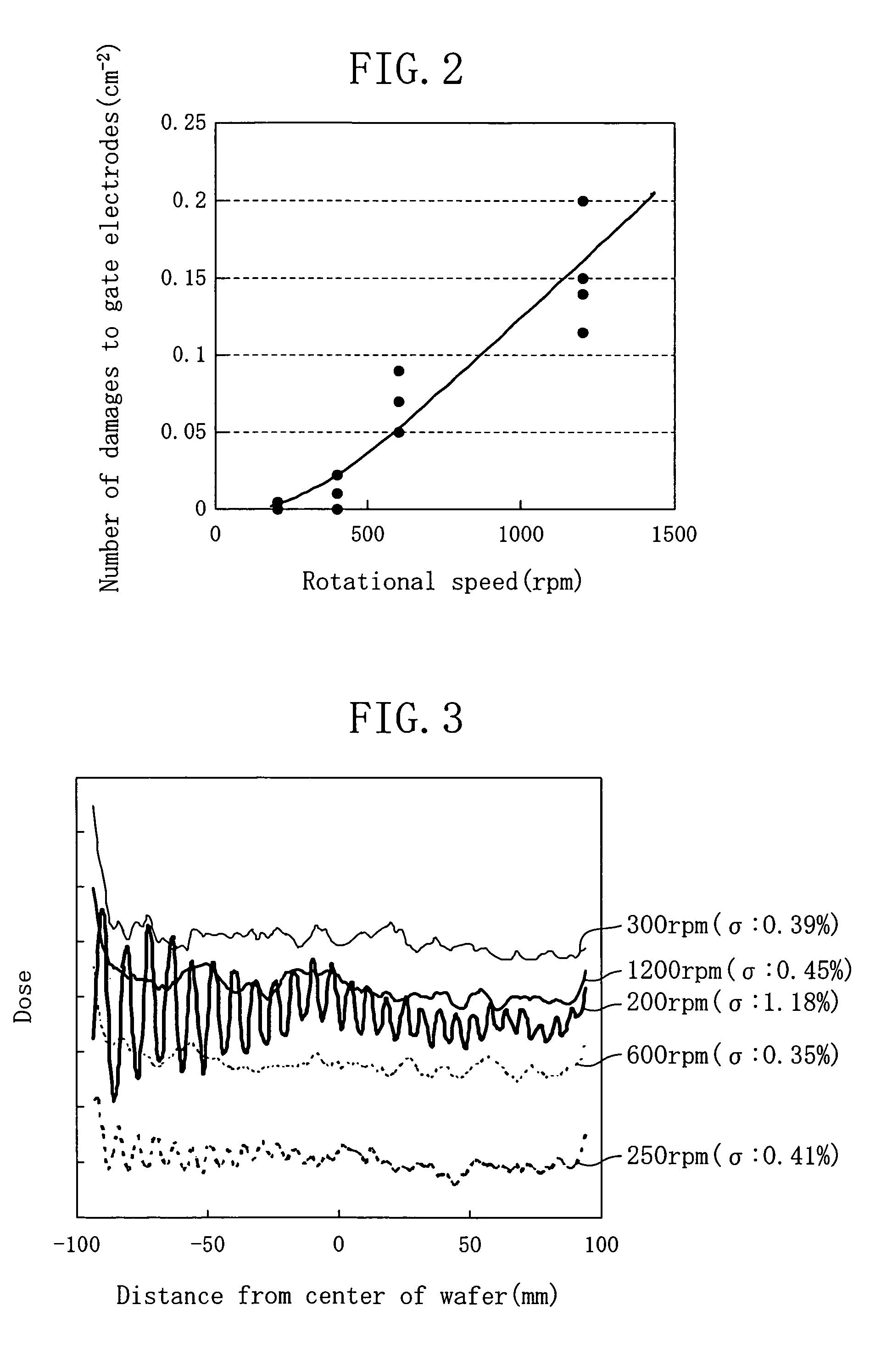
[0059]FIG. 1A is a plan view illustrating an end station part of an apparatus used for the substrate processing method of this embodiment, more specifically, an ion implantation apparatus. The end station part is placed in a processing container 210 allowed to have a high vacuum atmosphere during processing of the substrate. The apparatus is of a high-current type and a batch type, and its end station part comprises a dish-like large-diameter disk 200 on which a plurality of substrates 201 are placed so as to be fixed. The disk 200 can rotate about a rotational shaft 202 attached to its middle part.

[0060]FIG. 1B illustrates the state of the end station part during ion implantation when obliquely viewed. During ion implantation, the disk 200 is rotated at a predetermined rotation speed and linearly moved up and down. While the disk 200 is moving a...


PUM


Abstract

A substrate processing method of the present invention includes the steps of placing a substrate inside a vacuum container containing particles and processing the substrate inside the container while moving the substrate at a predetermined relative velocity of the substrate to the container. In this case, an allowable upper limit of the number or density of defects produced at the substrate due to the particles in the process for the substrate is determined, and the predetermined relative velocity is set at a value equal to or smaller than the relative velocity obtained when the number or density of defects reaches the upper limit.

Description

CROSS-REFERENCE TO RELATED APPLICATIONS[0001]The disclosure of Japanese Patent Application No. 2005-190011 filed on Jun. 29, 2005 including specification, drawings and claims is incorporated herein by reference in its entirety.BACKGROUND OF THE INVENTION[0002](1) Field of the Invention[0003]The present invention relates to substrate processing methods for fabrication of semiconductor integrated circuits or other purposes, and more particularly relates to substrate processing methods for processing substrates, e.g., implanting ions into substrates or cleaning substrates, while moving substrates at high speed.[0004](2) Description of Related Art[0005]With a higher degree of integration of semiconductor integrated circuit devices, the sizes of gate electrodes of metal oxide semiconductor (MOS) transistors are becoming finer and finer. This reduces the physical strengths of gate electrodes, and thus gate electrodes have come to easily suffer damage due to shock.[0006]In the case where s...

Claims


Application Information

Patent Timeline
Patent Type & Authority Patents(United States)
IPC IPC(8): H01L21/66
CPCH01L21/02057H01L21/67213H01L21/26513H01L21/265H01L21/425
Inventor KANEKO, TOSHIONISHIWAKI, TORU
Owner PANASONIC SEMICON SOLUTIONS CO LTD
Learn More