Substrate noise tool

a tool and substrate technology, applied in the field of substrate noise tools, can solve the problems of too late, the performance of sensitive analog circuits can be severely degraded, and the problem of substrate noise is more and more pronounced, so as to achieve fast simulation, accurate representation of substrate noise, and the effect of reducing noise coupling

Inactive Publication Date: 2009-01-20
MASSACHUSETTS INST OF TECH
View PDF6 Cites 16 Cited by
  • Summary
  • Abstract
  • Description
  • Claims
  • Application Information

AI Technical Summary

Benefits of technology

[0035]The problems of the prior art have been overcome using a software program and method for analyzing substrate noise, using a range of input information. Briefly, a substrate noise analysis tool is disclosed. This tool is capable of accepting inputs of increasing complexity and granularity, thus making the tool suitable for employment during all phases of IC design. During the early stages of design, the tool can accept coarse circuit descriptions, such as gate level netlists. The design tool is capable of generating rudimentary substrate models based on estimated die size. Using these inputs, a relatively fast simulation can be performed, allowing the designer to have an early indication of potential substrate noise issues. During the middle stages of design, the tool can accept more accurate circuit descriptions, such as a SPICE netlist. A more detailed substrate model, which considers layout information, can be generated. This simulation produces a more accurate representation of the substrate noise, thereby allowing the designer to make layout and circuit modifications if necessary before the circuit is completed. Lastly, during final verification, the tool can accept an even more accurate netlist, such as a SPICE netlist that includes parasitics. The tool can also accept a substrate model generated either by this design tool, or another substrate modeling tool, such as SubstrateStorm. The simulation based on these inputs is far more accurate than those above, and provides the substrate noise analysis necessary to allow the designer to determine whether the circuit should be fabricated.

Problems solved by technology

With the increasing levels of integration in today's integrated circuits and ever-increasing digital circuit speeds, the problem of substrate noise is more and more pronounced.
The performance of sensitive analog circuits can be severely degraded by excessive substrate noise.
However, this is often too late, for if the substrate noise negatively impacts the performance of the circuit, the circuit must be laid out again and re-fabricated.
This consumes valuable time and money.
Standard techniques to simulate expected substrate noise tend to be either accurate but extremely inefficient, or fast but rather inaccurate.
The inefficient techniques are accurate because all noise sources, coupling, and propagation mechanisms are well modeled; however, this leads to a large number of nodes in the simulation model.
This excessive number of nodes accounts for the temporal inefficiency.
In contrast, the fast techniques rely on the random nature of the noise generated.
Thus, detrimental noise components are often omitted or grossly underestimated.
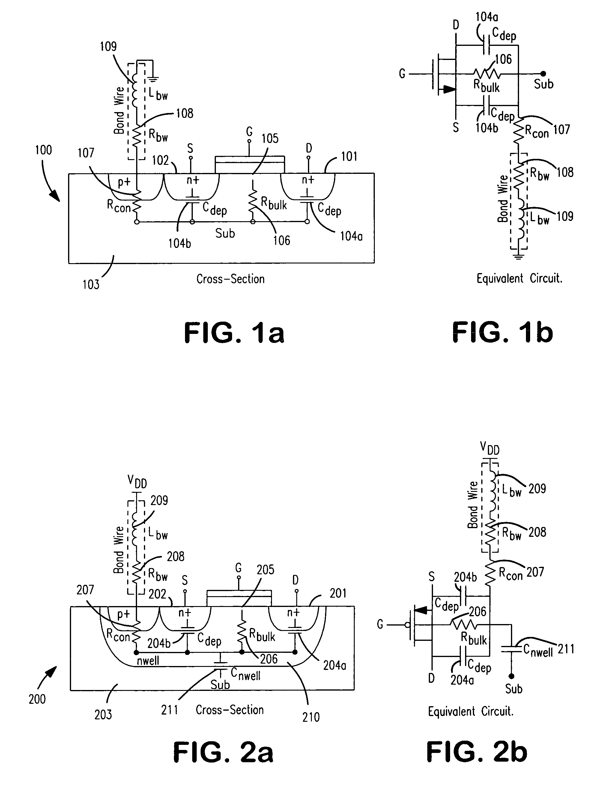
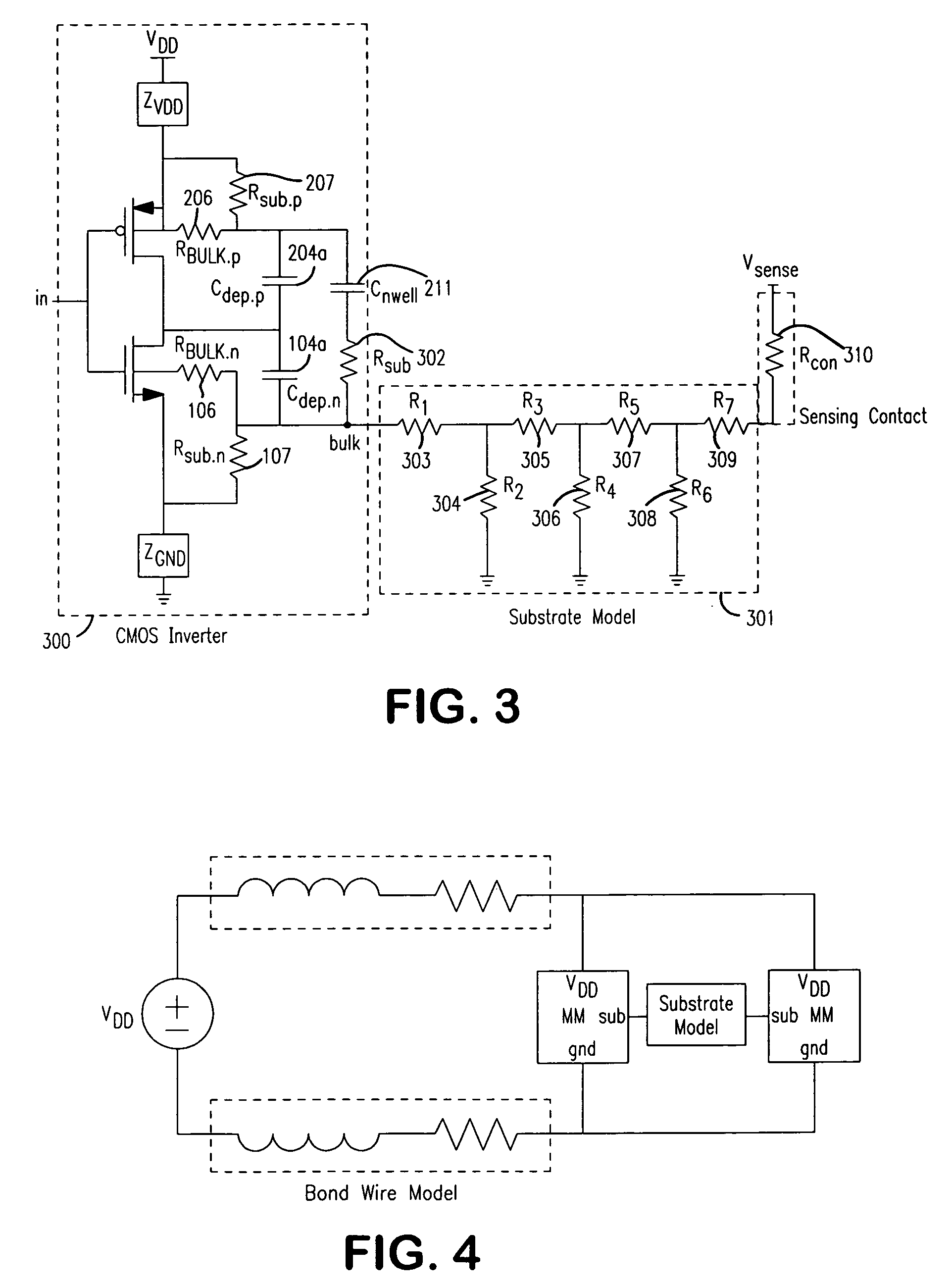
Different approaches to accurately model the substrate typically result in an extremely large mesh of passives.
Accurate substrate modeling is a very complex problem.
However, more rudimentary substrate models were developed to permit extremely fast substrate simulations at the expense of some accuracy.
Most work on radio frequency (RF) circuits has been limited to low noise amplifiers.
As described above, this approach yields the most accurate data, however it can be both time and computation intensive.
Because the complexity of the circuit scales rapidly with circuit size, the simulation time will be excessively long and in many cases will not converge.
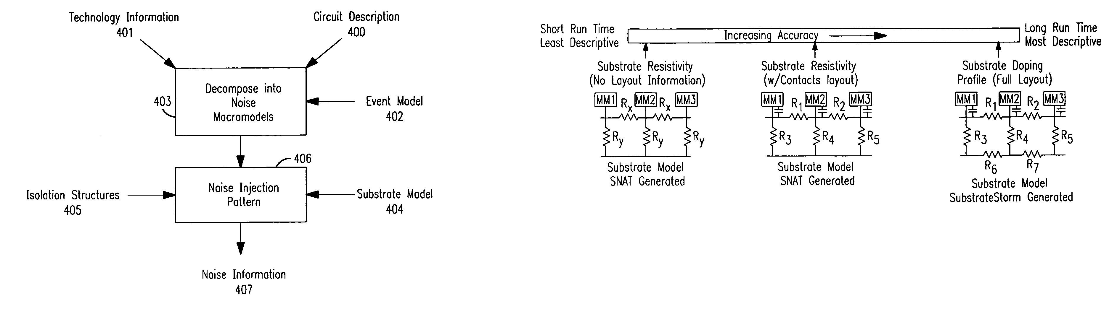
As described above, transistor level simulation techniques result in prohibitively long simulation times. If the noise behavior could be abstracted to a higher level while still preserving the relationship to the substrate, simulation times could be reduced.
Because mathematical expressions instead of real waveforms are used to generate the noise profiles, this methodology yields less accurate predictions of the substrate noise.
Furthermore, with technology scaling, mathematical models used to model transistor behavior are becoming more complex.
Because this technique relies on the ability of the mathematical expressions to model the substrate noise behavior, its accuracy will further diminish for future technology nodes.
These approaches yield very good accuracy with reasonable simulation times. The main limitation of the macromodelling technique is that determining the worst case noise behavior of the circuit can be a formidable task.
More and more digital systems are interconnect dominated, and in such circuits, the noise contribution from interconnect can be significant.
This technique cannot be used to examine the time varying nature of the substrate noise or to determine the frequency content of the noise.
Knowing only an estimate of the peak substrate noise value without knowing its frequency content is not entirely useful.
Without knowing the frequency content, the severity of the substrate noise problem cannot be assessed.
Furthermore, the amount of attenuation afforded by isolation structures is frequency dependent.
Without knowing what frequencies should be targeted, the isolation structure design will not be optimized.
Therefore, this technique can only be used to generate a rough estimate of the noise and thus is most useful for floorplanning.
A full SPICE transistor level simulation yields the most accurate results; however, it is impractical for most circuits as the run-time increases rapidly with circuit complexity.
The most common problem is that the noise macromodel does not completely encapsulate the noise behavior of the original circuit.
Furthermore, certain assumptions inherent in specific tools do not permit the tool for use with non-epi substrates.
Because a full layout is required, substrate noise simulation can only be performed at the end of the design cycle.
However, none of these are flexible enough to work at any stage in the design cycle.
Specifically, these tools can only be used for final verification.

Method used


Image

  • Substrate noise tool
  • Substrate noise tool
  • Substrate noise tool

Examples


Embodiment Construction

[0050]FIG. 5 illustrates a high-level block diagram showing the operation of the software program, which is written in Perl, although other computer languages are within the scope of the invention.

[0051]The software program requires several sets of input information: circuit information 400, technology information 401, an event model 402, optionally a substrate model 404, and optionally information concerning the isolation structures 405. Using the first two sets of information, the software program decomposes the circuit into equivalent noise macromodels 403. The noise macromodels together with the event model 402 for each node in the circuit are used to construct the noise signature 406. This noise signature 406 is then simulated with the substrate model 404 and power grid / isolation structures 405 to compute the substrate noise profile. The outputs 407 are a time domain representation and noise spectrum. Each of these components is described in more detail below.

[0052]As shown in ...


PUM


Abstract

System and method for analyzing substrate noise is disclosed, which is capable of accepting inputs of increasing complexity and granularity. During the early phases, the tool can accept coarse circuit descriptions, such as gate level netlists. The tool is capable of generating rudimentary substrate models based on estimated die size, allowing the designer to have an early indication of potential substrate noise issues. During the middle phases, the tool can accept more accurate circuit descriptions, such as a SPICE netlist. A more detailed substrate model can be generated, which considers layout information, thereby allowing the designer to make layout and circuit modifications before the circuit is completed. Lastly, during final verification, the tool can accept an even more accurate netlist, such as a SPICE netlist that includes parasitic capacitance. The tool can also accept a more detailed substrate model and provides the substrate noise analysis necessary to finalize the design.

Description

[0001]This application claims priority of U.S. Provisional application No. 60 / 718,471 filed Sep. 19, 2005, the disclosure of which is incorporated herein by reference.BACKGROUND OF THE INVENTION[0002]With the increasing levels of integration in today's integrated circuits and ever-increasing digital circuit speeds, the problem of substrate noise is more and more pronounced. The performance of sensitive analog circuits can be severely degraded by excessive substrate noise. The effect of substrate noise on the circuits within an IC is typically observed during the testing phase only after the chip has been fabricated. However, this is often too late, for if the substrate noise negatively impacts the performance of the circuit, the circuit must be laid out again and re-fabricated. This consumes valuable time and money. Therefore, a determination of substrate noise coupling during the design phase would be extremely beneficial to circuit designers who can incorporate the effect of the n...

Claims


Application Information

Patent Timeline
Patent Type & Authority Patents(United States)
IPC IPC(8): G06F17/50
CPCG06F17/5036G06F30/367
Inventor CHECKA, NISHACHANDRAKASAN, ANANTHAREIF, RAFAEL
Owner MASSACHUSETTS INST OF TECH
Why Eureka
Try Eureka