
In-plane switching liquid crystal display device

a liquid crystal display and switching technology, applied in non-linear optics, instruments, optics, etc., can solve the problems of insufficient rubbing of the sloping area of the insulation film b>9/b>, easy rubbing of the falling sloping area to be less adequate, and difficult control of the orientation of the liquid crystal material in the region. , to achieve the effect of low black brightness and high numerical apertur

Active Publication Date: 2009-01-27
NEC LCD TECH CORP
View PDF6 Cites 5 Cited by
  • Summary
  • Abstract
  • Description
  • Claims
  • Application Information

AI Technical Summary

Benefits of technology

"The present invention provides a high-contrast in-plane switching type liquid crystal display device with a high numerical aperture and low black brightness in a multi-domain system. This is achieved by forming a shielding layer in a region that includes the entire region directly over the insulation film and in a region positioned inside the region directly over the electrode. This blocking of light by the shielding layer results in a high-contrast display with low black brightness."

Problems solved by technology

The following problems existed in the conventional technology described above.
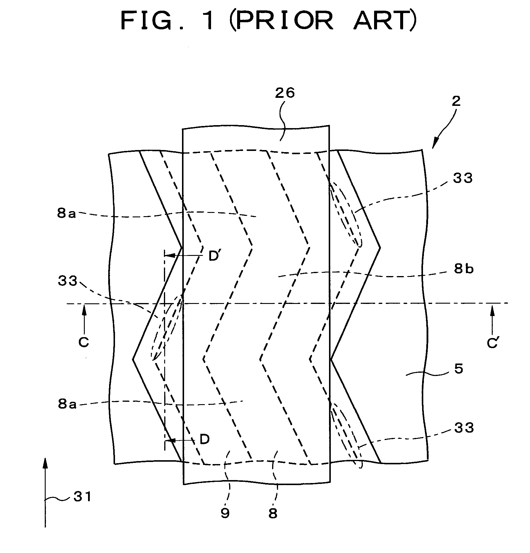
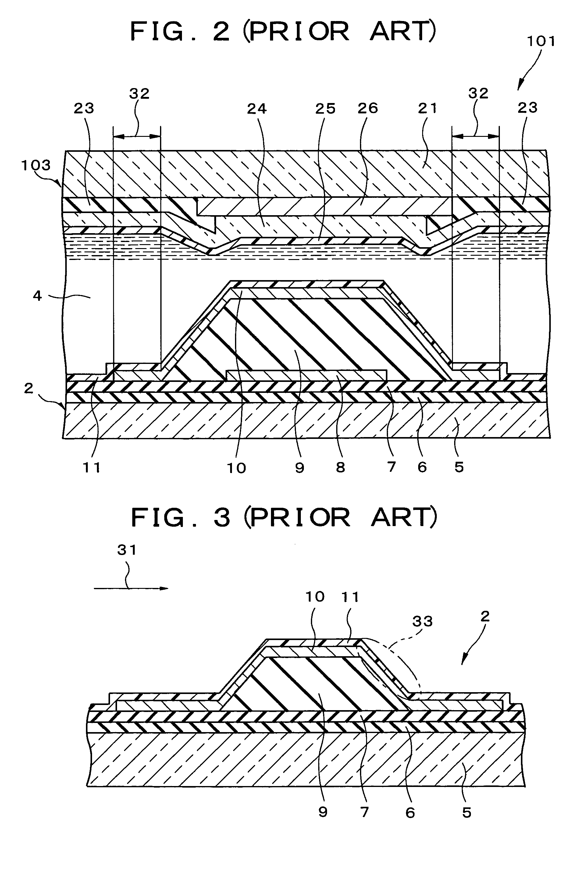
Because of this, the sloping area of the insulation film 9 does not have sufficient rubbing in the rubbing process of the oriented film 11 while manufacturing a liquid crystal display device.
In particular, it is easier for the rubbing of the falling sloping area to be less adequate than the rising sloping area.
Therefore, it is difficult to control the orientation of the liquid crystal material in the region 33.
Moreover, if the rubbing strength is unreasonably increased in order to improve the orientation force of the oriented film 11, the oriented film 11 will not be able to bear the rubbing and detach.

Method used


Image

  • In-plane switching liquid crystal display device
  • In-plane switching liquid crystal display device
  • In-plane switching liquid crystal display device

Examples


Embodiment Construction

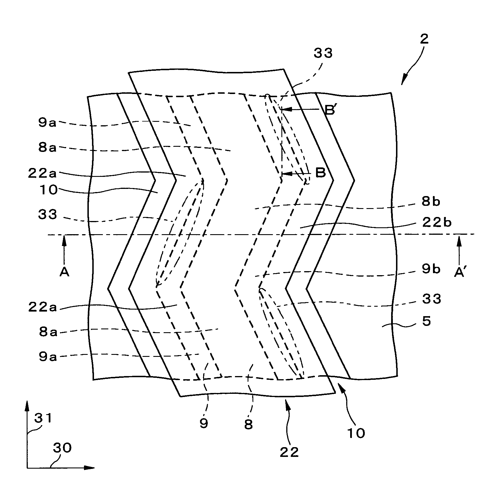
[0025]In the following, a detailed description of the embodiment of the present invention will be described referring to the drawings. FIG. 4 is a plan view showing the liquid crystal display device according to the embodiment of the present invention. FIG. 5 is a partially enlarged plan view showing a region 34 shown in FIG. 4. FIG. 6 is a cross-sectional view taken along the line A-A′ shown in FIG. 5 and FIG. 7 is a cross-sectional view taken along the line B-B′ shown in FIG. 5. FIG. 4 and FIG. 5 only show the active element substrate and do not show the opposing substrate. FIG. 5 does show the shielding layer. The liquid crystal display device shown in FIG. 4 to FIG. 7 is a multi-domain system in-plane switching type liquid crystal display device and is a normally black type liquid crystal display device. In the liquid crystal display device according to the embodiment, an active element substrate 2 and an opposing substrate 3 are provided parallel to each other and a liquid crys...


PUM

PropertyMeasurementUnit
sizeaaaaaaaaaa
shapeaaaaaaaaaa
electric fieldsaaaaaaaaaa

Abstract

A data wiring is provided on a glass substrate in an active element substrate. For the data wiring, a first portion, extending in a direction that slopes and forms a fixed angle with respect to the rubbing direction of an oriented film, and a second portion, extending in a direction sloping to the opposite side of the first portion are alternately arranged and formed in a zigzag pattern. A convex insulation film is formed in a zigzag pattern to cover the data wiring and a common electrode is formed in a zigzag pattern to cover the insulation film. A shilding layer is formed in a zigzag pattern on an opposing substrate to completely cover the insulation film and does not protrude from the region directly above the common electrode. The high-contrast, multi-domain system in-plane switching type liquid crystal display device obtained with a high numerical aperture and low black brightness.

Description

BACKGROUND OF THE INVENTION[0001]1. Field of the Invention[0002]The present invention relates to multi-domain system in-plane switching type liquid crystal display device.[0003]2. Description of the Related Art[0004]Conventionally, multi-domain systems have been developed for in-plane switching type liquid crystal display devices (for example, refer to Japanese Patent Laid-Open Publication No. 2002-323706, FIG. 15 and FIG. 47 as well as Japanese Patent Laid-Open Publication No. 2002-258321, FIG. 8). A multi-domain system is a system in which pixel electrodes and common electrodes, formed on an active element substrate, are formed in a zigzag shape to form one pair of sub-pixel regions (domain) on each unit pixel. In other words, a first portion, extending in a direction sloping towards the rubbing direction of an oriented film, and a second portion, extending in a direction sloping on the opposite side of the first portion towards that rubbing direction, are alternately arranged on ...

Claims


Application Information

Patent Timeline
Patent Type & Authority Patents(United States)
IPC IPC(8): G02F1/1343
CPCG02F1/133345G02F1/133512G02F1/134363G02F1/1362
Inventor ITO, HIDEKIINOUE, DAISUKEKAMINO, TAKASHITANAKA, HIROMITSU
Owner NEC LCD TECH CORP
Learn More