
Pixel electrode and liquid crystal display panel

a liquid crystal display panel and pixel electrode technology, applied in non-linear optics, instruments, optics, etc., can solve the problem of color shift under large view angle and other problems, and achieve the effect of reducing the demand for backlight brightness, reducing the cost and usage power consumption, and increasing penetration ra

Inactive Publication Date: 2017-07-06
SHENZHEN CHINA STAR OPTOELECTRONICS TECH CO LTD
View PDF12 Cites 3 Cited by
  • Summary
  • Abstract
  • Description
  • Claims
  • Application Information

AI Technical Summary

Benefits of technology

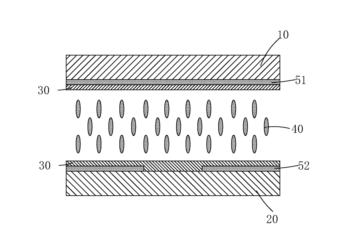
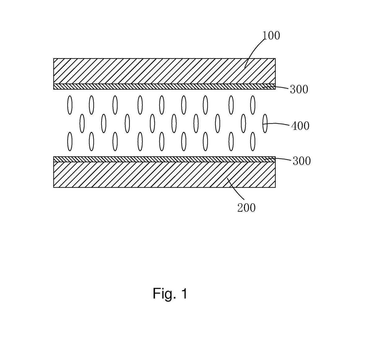
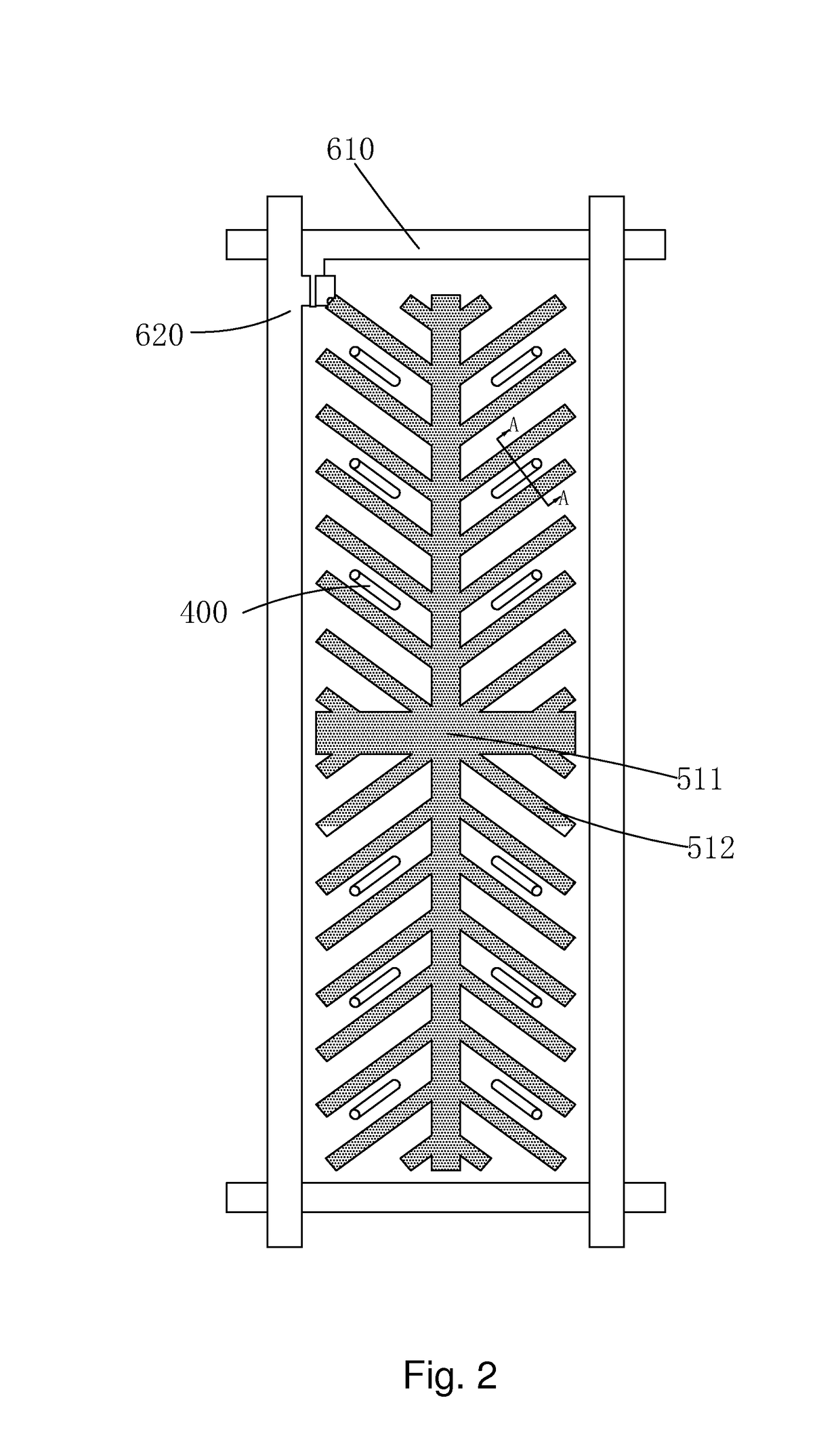
The present invention aims to provide a pixel electrode that can improve liquid crystal display panels' penetration rate and reduce the demand for backlight brightness, thus reducing costs and power consumption. The technical effect is achieved through a design that includes two areas in one sub pixel and eliminates the need for a keel or one keel, which can cause liquid crystal molecules to fall in the incorrect directions.

Problems solved by technology

However, because the VA liquid crystal display utilizes vertical twist liquid crystals and the birefraction difference of the liquid crystal molecules is larger, the issue of the color shift under large view angle is more serious.

Method used


Image

  • Pixel electrode and liquid crystal display panel
  • Pixel electrode and liquid crystal display panel
  • Pixel electrode and liquid crystal display panel

Examples


first embodiment

[0056]FIG. 5 shows the pixel electrode according to the present invention. The frame 1 comprises a first frame electrode 11 and a third frame electrode 13 which are mutually parallel, and a second frame electrode 12 which is orthogonally connected with end portions of the first frame electrode 11 and the third frame electrode 13; lengths of the first frame electrode 11 and the third frame electrode 13 are equal, and a length of the second frame electrode 12 is larger than the lengths of the first frame electrode 11 and the third frame electrode 13.

[0057]The plurality of first branch electrodes 21, the plurality of second branch electrodes 22 are positioned in an area surrounded by the first, second, third frame electrodes 11, 12, 13; the plurality of first branch electrodes 21 and the plurality of second branch electrodes 22 are symmetric relative to a midnormal of the first, third frame electrodes 11, 13.

[0058]Preferably, widths of the first, second, third frame electrodes 11, 12, ...

second embodiment

[0063]In the second embodiment, the plurality of first branch electrodes 21, the plurality of second branch electrodes 22 respectively correspond to upper, lower, two areas in one sub pixel, and design of not including the keel is utilized, and the active area in enlarged to solve the issue that the penetration rate is low because the liquid crystal molecules at the structure of the (cross) keel of pozidriv pixel electrode fall down toward the improper directions, to raise the penetration rate for reducing the demand to the backlight brightness of the liquid crystal display panel and lowering the cost and the usage power consumption.

third embodiment

[0064]FIG. 7 shows the pixel electrode according to the present invention. The frame 1 comprises a first frame electrode 11, and a second frame electrode 12 orthogonally connected with the middle of the first frame electrode 11; a length of the second frame electrode 12 is smaller than a length of the first frame electrode 11.

[0065]The plurality of first branch electrodes 21, the plurality of second branch electrodes 22 are respectively positioned at one side of the first frame electrode 11 and in two areas divided by the second frame electrode 12; the plurality of first branch electrodes 21 and the plurality of second branch electrodes 22 are symmetric relative to the second frame electrode 12.

[0066]Preferably, widths of the first, second frame electrodes 11, 12 and widths of the first, second branch electrodes 21, 22 are the same.

[0067]In the third embodiment, the plurality of first branch electrodes 21, the plurality of second branch electrodes 22 respectively correspond to upper...


PUM


Abstract

The present invention provides a pixel electrode and a liquid crystal display panel. The pixel electrode comprises a frame (1), a plurality of first branch electrodes (21) which are parallel with one another and spaced with one another, and a plurality of second branch electrodes (22) which are parallel with one another and spaced with one another; the frame (1) comprises a plurality of frame electrodes which are connected with one another, and the plurality of first branch electrodes (21), the plurality of second branch electrodes (22) respectively appear 45° include angles with the plurality of frame electrodes, and the plurality of first branch electrodes (21) and the plurality of second branch electrodes (22) are orthogonal. The pixel electrode comprises two areas in one sub pixel, and utilizes design of not including the keel or one keel, and the active area in enlarged and the penetration rate of the liquid crystal panel is raised. In the liquid crystal display panel of the present invention, the pixel electrode comprises two areas in one sub pixel, and utilizes design of not including the keel or one keel, and the penetration rate is higher, and the demand to the backlight brightness is lower, and the usage power consumption is lower.

Description

FIELD OF THE INVENTION[0001]The present invention relates to a display technology field, and more particularly to a pixel electrode and a liquid crystal display panel.BACKGROUND OF THE INVENTION[0002]In recent years, the Thin Film Transistor-LCD (TFT-LCD) has been rapidly developed and applied widely. For the TFT-LCD in the mainstream market, three types, which respectively are Twisted Nematic (TN), Super Twisted Nematic (STN), In-Plane Switching (IPS) and Vertical Alignment (VA) can be illustrated. The VA liquid crystal display possesses extremely high contrast than the liquid crystal displays of other types, which can reach up to 4000-8000 in general. It has very wide application in large scale display, such as television or etc.[0003]The reason why the VA liquid crystal display possesses extremely high contrast is that the liquid crystal molecules are vertically aligned to the substrate surface, and no phase difference exists, and light leakage is very small, and the dark state b...

Claims


Application Information

Patent Timeline
IPC IPC(8): G02F1/1343G02F1/1362G02F1/1368
CPCG02F1/134309G02F1/13439G02F2201/121G02F1/136286G02F2201/123G02F1/1368G02F1/133707G02F1/134336
Inventor ZHONG, XINHUI
Owner SHENZHEN CHINA STAR OPTOELECTRONICS TECH CO LTD
Learn More