Workpiece processing device

a processing device and workpiece technology, applied in the direction of mechanical control devices, process and machine control, instruments, etc., can solve the problems of inability to appropriately set the operating condition of the dicing device according to the bar code, error occurs when the character information on the wafer is read, and the optical reading device cannot accurately read out the character information of the wafer. to prevent the failure of adhering to the peeling tape

Active Publication Date: 2009-02-17
TOKYO SEIMITSU
View PDF23 Cites 0 Cited by
  • Summary
  • Abstract
  • Description
  • Claims
  • Application Information

AI Technical Summary

Benefits of technology

[0015]In the first aspect, after the surface protection film has been peeled from the wafer on the support table, without releasing the suction operation of the workpiece, the bar code adhering operation is conducted on the workpiece on the same support table. That is, it is not necessary to move the workpiece from the support table to another support table between the surface protection film peeling operation and the bar code adhering operation. Since the support table is not changed, it is possible to prevent the workpiece from undulating. As a result, the bar code can be appropriately adhered to the workpiece. Accordingly, it is possible to avoid failures when adhering the bar code. In this connection, the terminology of the workpiece includes both a single body of a wafer and a body in which the wafer and the mount frame are integrated with each other by the dicing tape.
[0017]In the second aspect, it is possible to avoid failures in reading character information on the wafer.
[0019]In the third aspect, after the workpiece has been cleaned by the cleaning means, the surface protection film is peeled. Due to the foregoing, the adhesive force between the peeling tape and the surface protection film is enhanced, so that failure of adhering the peeling tape can be prevented.

Problems solved by technology

When the dicing tape and / or wafer 20 slightly undulates, it is impossible for the optical reading device to accurately read out the character information of the wafer.
Accordingly, an error occurs when the character information on the wafer is read.
In this case, in the dicing step, which is an after-step, it is impossible to appropriately set the operating condition of the dicing device according to the bar code.
As a result, yield is lowered or working time is delayed.

Method used


Image

  • Workpiece processing device
  • Workpiece processing device
  • Workpiece processing device

Examples


Embodiment Construction

[0029]Referring to the accompanying drawings, an embodiment of the present invention will be explained below. Like reference numerals are used to indicate like parts in the following drawings. In order to facilitate understanding, the reduced scale used in these drawings has been appropriately changed.

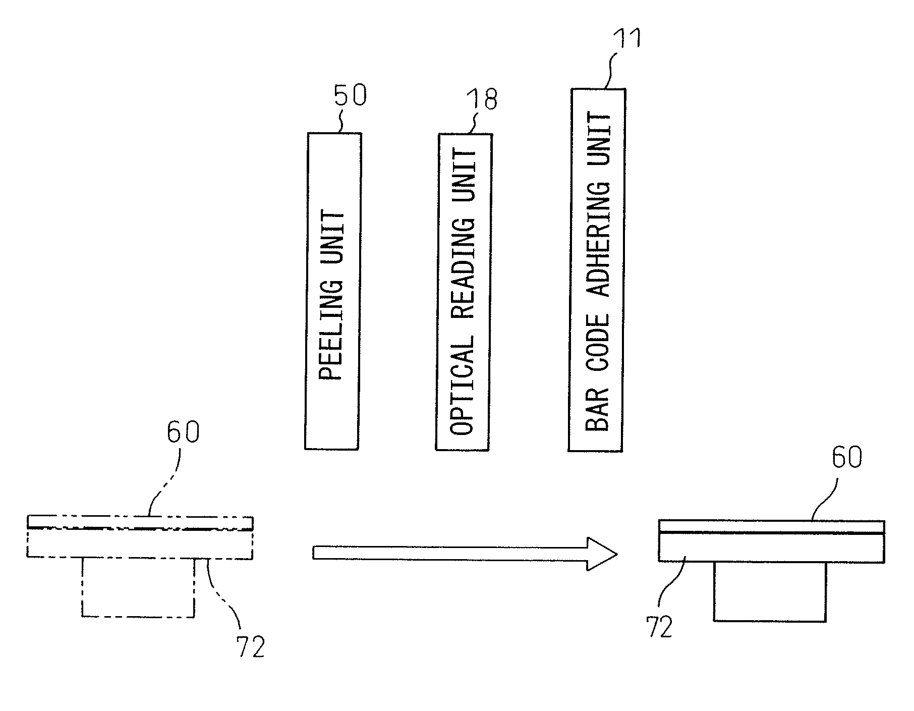
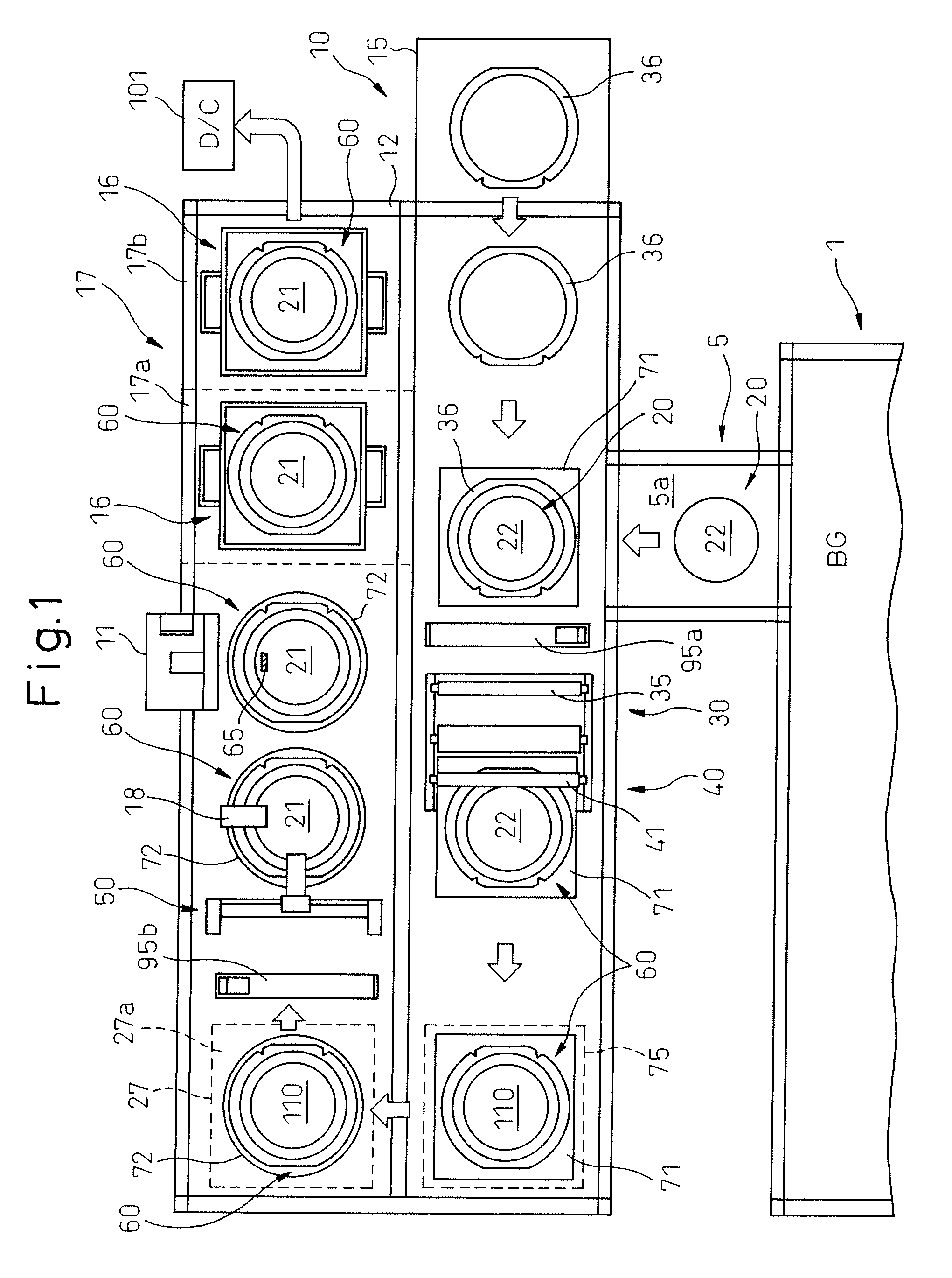
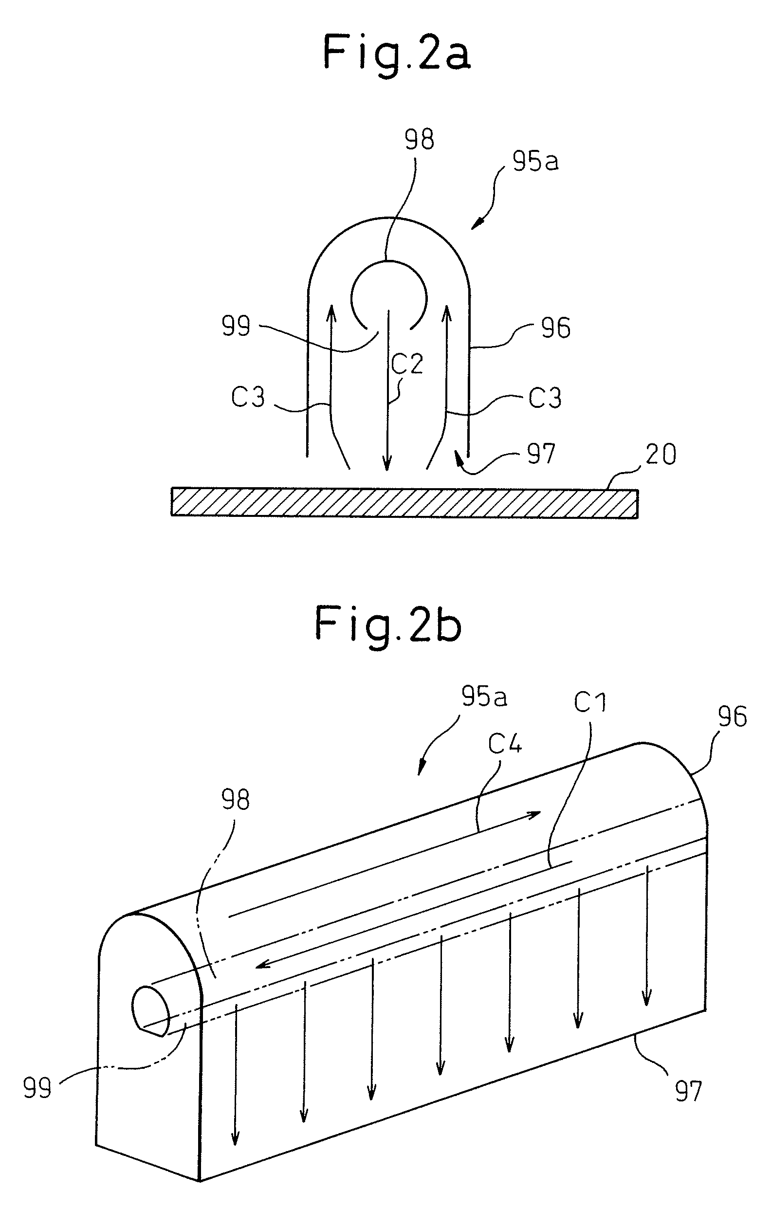
[0030]FIG. 1 is a plan view showing a wafer processing device according to the present invention. In FIG. 1, a wafer processing device 10 is arranged adjacent to a back-grinder 1. As shown in FIG. 1, this wafer processing device 10 is connected to the back-grinder 1 by a first UV irradiation portion 5 (ultraviolet ray irradiation portion).

[0031]In a housing 12 of the wafer processing device 10 shown in FIG. 1, a mount frame arrangement portion 15, in which a plurality of mount frames 36 are arranged, is provided. In this housing 12, a cassette region 17 for a cassette 16, in which wafers 20 integrated with the mount frames 36 are accommodated, is arranged adjacent to the mount frame ar...


PUM

PropertyMeasurementUnit
thicknessaaaaaaaaaa
opticalaaaaaaaaaa
optical readingaaaaaaaaaa

Abstract

A workpiece processing device (10) for processing a workpiece (60; 20, 36) comprises: a surface protection film peeling means (50) for peeling a surface protection film (110), which is adhered to a front surface (21) of a workpiece, with a peeling tape (4); a bar code adhering means (11) for adhering a bar code (65) corresponding to the workpiece to the workpiece; and a movable support table (72) for supporting the workpiece. A peeling operation for peeling the surface protection film conducted by the surface protection film peeling means and a adhering operation for adhering a bar code conducted by the bar code adhering means are given to the workpiece while the workpiece is being supported by the support table. Due to the foregoing, it is possible to avoid failures when adhering the bar code to the workpiece, such as a wafer. The bar code adhering means may adhere the bar code, which corresponds to character information of the workpiece read out by an optical reading means, to the workpiece.

Description

CROSS-REFERENCE TO RELATED APPLICATION[0001]This application claims priority of Japanese Patent Application Number 2006-155921, filed on Jun. 5, 2006.BACKGROUND OF THE INVENTION[0002]1. Field of the Invention[0003]The present invention relates to a workpiece processing device for processing a wafer workpiece, on the front surface of which a circuit pattern is formed and a surface protection tape is adhered, integrated with a mount frame into one body by a dicing tape.[0004]2. Description of the Related Art[0005]In the field of manufacturing semiconductors, there is a tendency for large-sized wafers to be used year after year. Further, in order to enhance packing density, wafer thickness is reduced. In order to reduce the wafer thickness, back-grinding is conducted on the back surface of a semiconductor wafer. At the time of back-grinding, in order to protect a semiconductor element formed on the front surface of a wafer, a surface protection film is adhered to the front surface of t...

Claims


Application Information

Patent Timeline
Patent Type & Authority Patents(United States)
IPC IPC(8): H01L21/67H01L21/673H01L21/677H01L21/68
CPCH01L21/67132H01L21/67294Y10T156/1906Y10S438/976Y10T156/1105Y10T156/1978Y10S414/135Y10T156/17H01L21/00H01L21/02
Inventor KAWASHIMA, ISAMUSATO, HIDESHIKINO, HIDEOAMETANI, MINORU
Owner TOKYO SEIMITSU
Why Eureka
Try Eureka