
Methods of packing user logical RAM into dedicated RAM blocks and dual-use logic/RAM blocks

Inactive Publication Date: 2009-02-17
ALTERA CORP
View PDF5 Cites 15 Cited by
  • Summary
  • Abstract
  • Description
  • Claims
  • Application Information

AI Technical Summary

Benefits of technology

[0012]It is an object of this invention to provide RAM mapping algorithms for shared blocks of memory at later stages of the Computer Aided Design (CAD) flow because RAM mapping at later stages of the CAD flow can take advantage of more accurate information about the device utilization and performance that is obtained following synthesis and make more intelligent mapping decisions.
[0014]RAM technology mapping during synthesis initially determines how user logical RAMs are implemented. This mapping may be based on estimates of memory and logic usage. This invention preferably performs RAM re-mapping at a later stage of the CAD flow in order to improve density and performance.

Problems solved by technology

With current larger devices, it would be impractical to attempt to lay out the logic without such software.
However, all of these conventional devices lacked LUT RAM capability—i.e., the ability to use LUTs to implement user logical RAM.
Furthermore, no known memory mapping algorithms perform optimization on shared blocks of logic and memory following the mapping that occurs during synthesis.

Method used


Image

  • Methods of packing user logical RAM into dedicated RAM blocks and dual-use logic/RAM blocks
  • Methods of packing user logical RAM into dedicated RAM blocks and dual-use logic/RAM blocks
  • Methods of packing user logical RAM into dedicated RAM blocks and dual-use logic/RAM blocks

Examples


Embodiment Construction

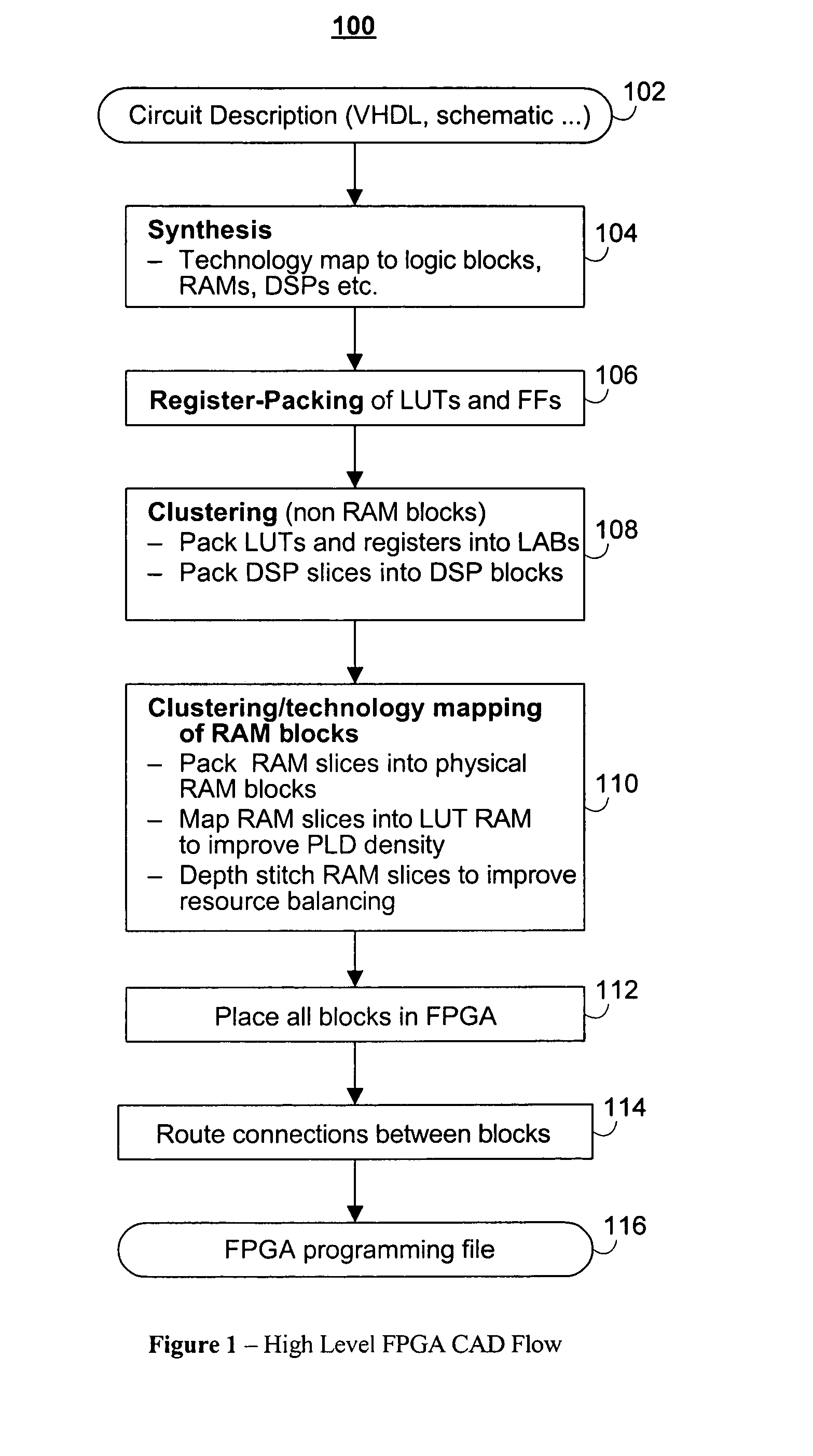
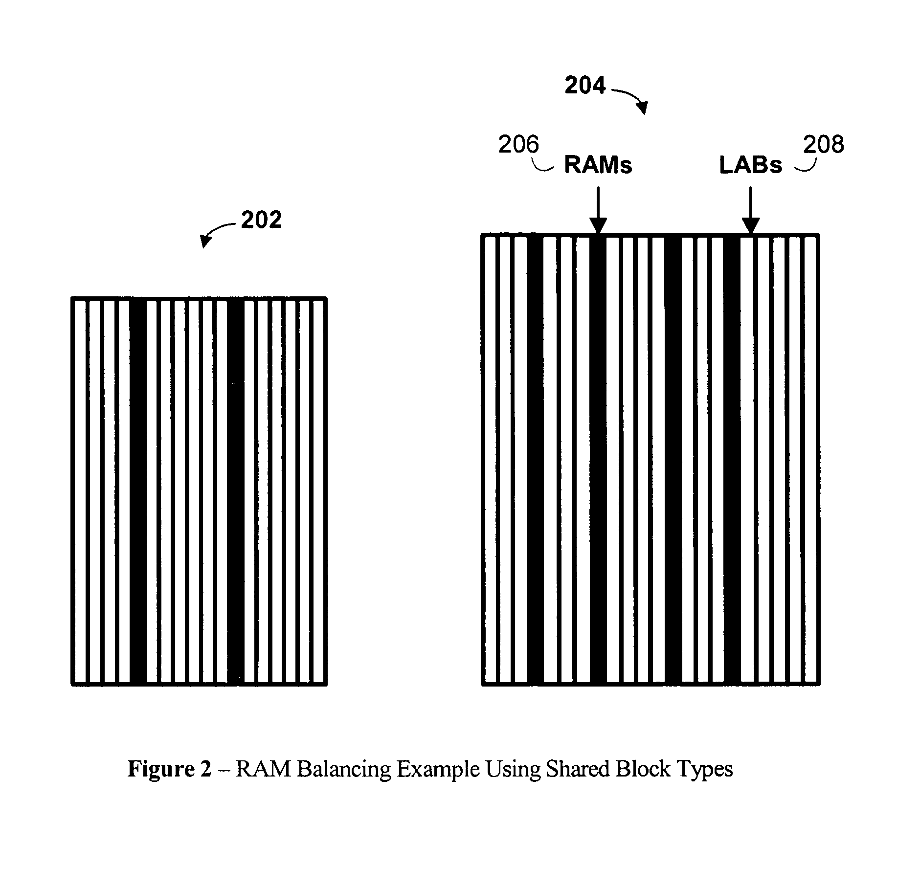
[0025]The objective of this invention is to optimize the utilization of memory block types that can support shared block types. This invention defines a method for mapping user logical RAMs into multiple types of physical RAMs as well as Look-Up Table (LUT) RAMs. LUT RAM is an example of a shared block type and is defined as a basic functional block that can implement both logic and memory operations.

[0026]Most functional blocks are only capable of implementing one type of operation. Such functional blocks which are capable of implementing one type of operation include a register, a logic element, input / output (I / O) or some other type. Other functional blocks, such as a LUT RAM, that have the ability to support multiple operations add complexity to the design flow. This complexity requires additional attention.

[0027]Traditionally, the design synthesis determines the mapping of the set of boolean equations representing the user circuit into basic logic elements (BLEs) and other funct...


PUM


Abstract

A method for technology mapping user logical RAM on a programmable logic device is provided. The method preferably includes clustering non-RAM functional block types in the programmable logic device. Following synthesis of a user design, the method then includes determining the number of physical RAM locations available on the selected device. Also, the method includes determining the number of physical RAM locations available in the PLD and the number of Look-Up-Table (LUT) RAM locations available in the PLD. Finally, the method includes determining a combination of physical RAM locations and LUT RAM locations for implementation of the user logical RAM. The combination preferably represents a beneficial combination of physical RAM and LUT RAM with respect to a predetermined metric.

Description

BACKGROUND OF THE INVENTION[0001]The present invention relates to implementing a user logic design in a programmable logic device (PLD or, alternatively, FPGA), and more particularly, the present invention relates to implementing logic design memory in blocks that share logic and memory and physical memory devices of a programmable logic device.[0002]Programmable logic devices are well known. Early programmable logic devices were one-time configurable. For example, configuration may have been achieved by “blowing” (i.e., opening) fusible links. Alternatively, the configuration may have been stored in a programmable read-only memory. Those devices generally provided the user with the ability to configure the devices for “sum-of-products” (or “P TERM”) logic operations. Later, such programmable logic devices incorporating erasable programmable read-only memory (EPROM) for configuration became available, allowing the devices to be reconfigured.[0003]Still later, programmable logic devi...

Claims


Application Information

Patent Timeline
IPC IPC(8): G06F17/50
CPCG06F17/5054G06F30/34
Inventor AHMED, ELIASPADALIA, KETAN
Owner ALTERA CORP
Features
  • Generate Ideas
  • Intellectual Property
  • Life Sciences
  • Materials
  • Tech Scout
  • Unparalleled Data Quality
  • Higher Quality Content
  • 60% Fewer Hallucinations
Learn More