Apparatus and method for responding to data retention loss in a non-volatile memory unit using error checking and correction techniques

Active Publication Date: 2009-02-24
TEXAS INSTR INC
View PDF5 Cites 1 Cited by
  • Summary
  • Abstract
  • Description
  • Claims
  • Application Information

AI Technical Summary

Benefits of technology

[0006]The aforementioned and other features are accomplished, according to the present invention, by providing the main memory with error checking and correction apparatus and with apparatus identifying a signal group error, detected by the error checking and correction apparatus, as a the result of a failing bit position in the main memory or the error checking and correction memory. A failing bit position occurs in a non-volatile main memory implemented, for example, in flash technology when charge leakage changes the state of original or default state of the bit location. When a correctable data signal group error is identified in a read operation, the error is corrected and the data signal group is forwarded to the central processing unit. In addition, the address and the location of the location of the error are stored. An interrupt flag is available to the central processing unit. When the central processing unit can be interrupted, the central processing unit restores the location in the main memory where the error originated based on the stored address and location. The error correcting apparatus will thereafter not be burdened with correcting errors in the same bit location. Additionally, it is sometimes desirable to leave unprogrammed locations in the memory where tables can be updated without erasing the location contents. When the existing table is to be updated, the old information is programmed to be all logic “0”s. The corresponding correction bits are programmed to be all logic “0”s. The new table with its new correction bits is then programmed into new, usually successive locations that were previously all logic “1”s (all erased bits). To facilitate this requirement, additional circuitry is added to suppress optionally error corrections when the data and the correction bits are all in the logic “1”s or logic “0”s state.
[0007]Other features and advantages of the present invention will be more clearly understood upon reading of the following description and the accompanying drawings and claims.

Problems solved by technology

Additionally, it is sometimes desirable to leave unprogrammed locations in the memory where tables can be updated without erasing the location contents.

Method used


Image

  • Apparatus and method for responding to data retention loss in a non-volatile memory unit using error checking and correction techniques
  • Apparatus and method for responding to data retention loss in a non-volatile memory unit using error checking and correction techniques
  • Apparatus and method for responding to data retention loss in a non-volatile memory unit using error checking and correction techniques

Examples


Embodiment Construction

.

1. Detailed Description of the Drawings

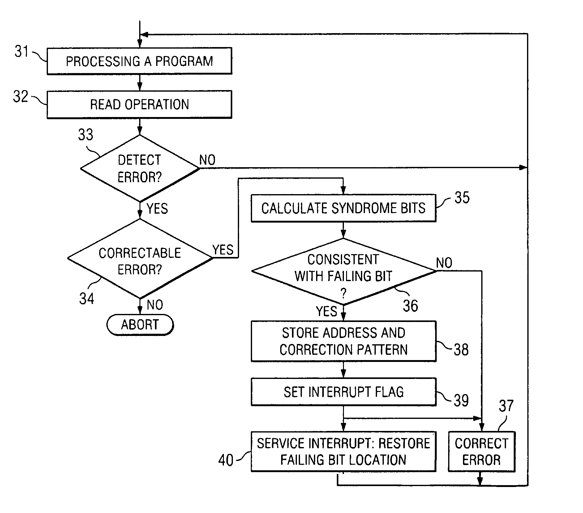
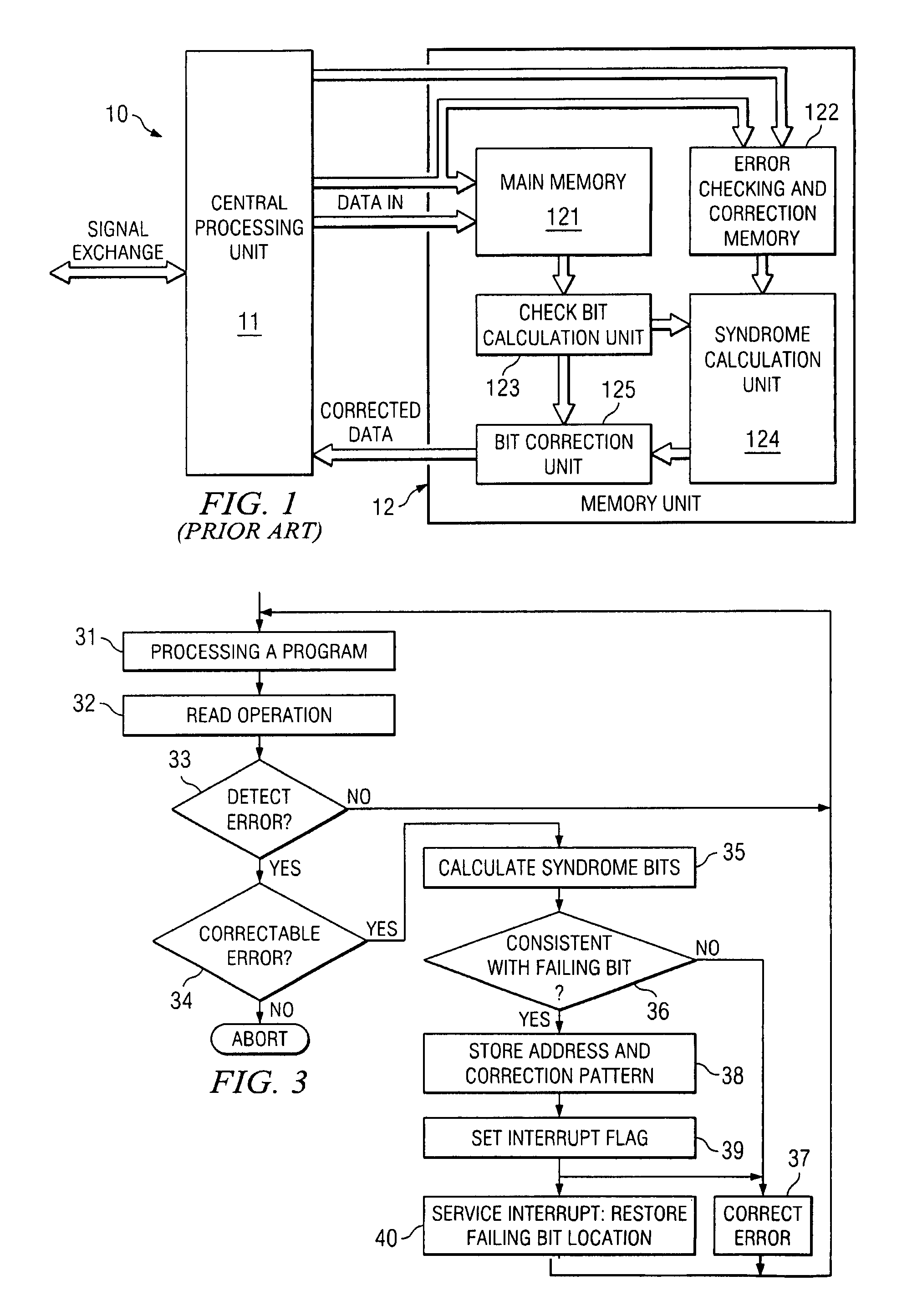
[0011]FIG. 1 has been described with respect to the related art.

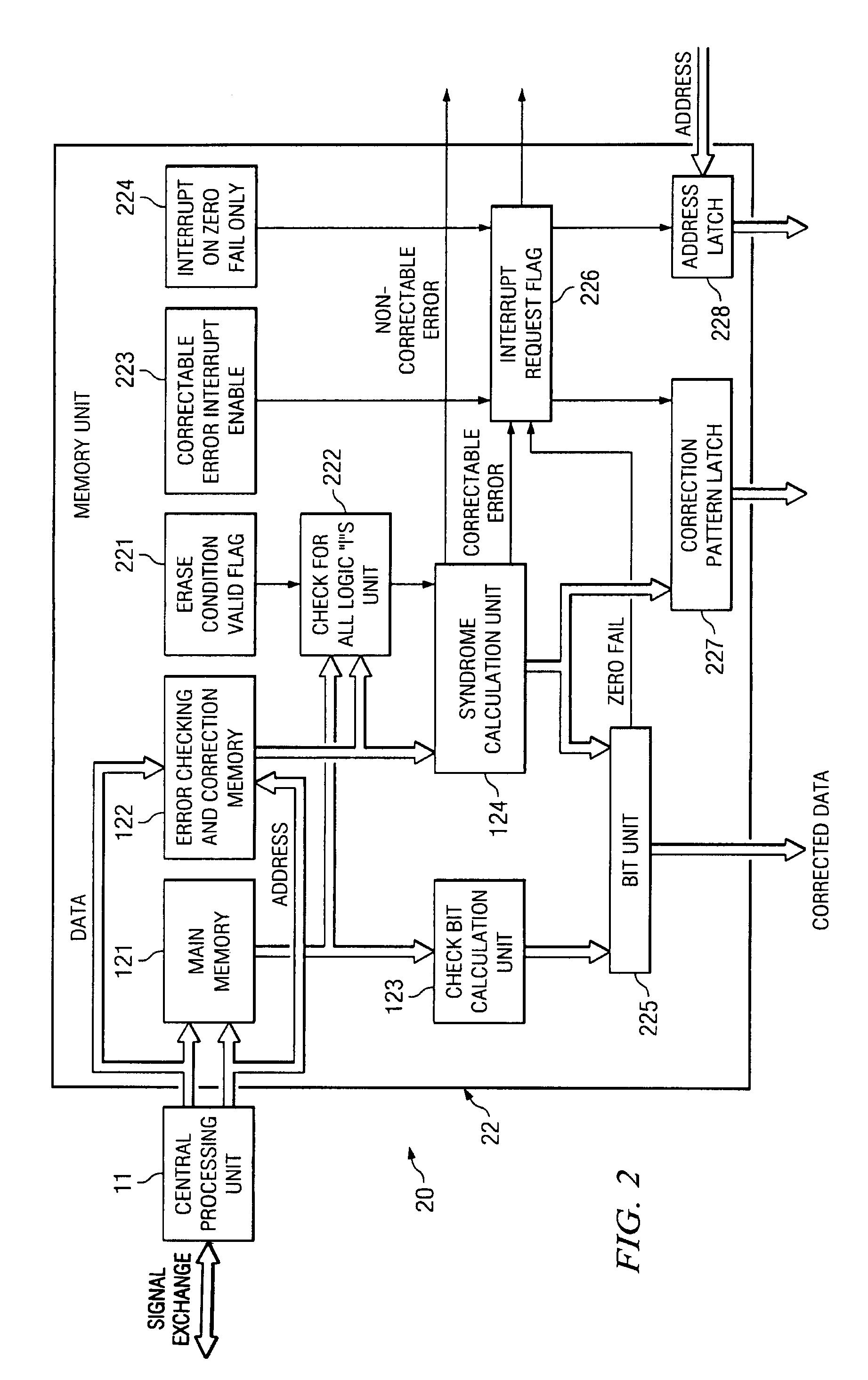
[0012]Referring next to FIG. 2, a block diagram of data processing system 20 according to the present invention is illustrated. The central processing unit 11, the main memory unit 121, the error checking and correction memory 122, and the syndrome calculation unit 124 perform essentially the same functions as described in FIG. 1. The bit correction unit 225 has an additional function as compared to the bit correction unit 125 of FIG. 1. In particular, when the bit location that is failing displays a logic “1” as compared to a correct logic “0”, an interrupt request flag indicative of a failing zero bit position is generated. The present invention has three control signals that are illustrated by the erase condition valid flag 221, the correctable error interrupt enable 223, and the interrupt on zero fail only 224. These control signals are applied to the interrupt flag request un...


PUM


Abstract

In a non-volatile memory unit such as a flash memory unit, the degradation of charge can result in an error during a read operation. By using the error checking and correction techniques, a determination can be made whether a detected error can be corrected and, if correctable, is the consistent with charge degradation at that bit position displaying the error. When a correctable error is detected, the signal group address and the correction pattern are stored and an interrupt request flag applied to the central processing unit. When the interrupt flag is processed, the central processing unit, using the signal group address and the correction pattern, restores the charge of the bit position in the memory unit. In this manner, further read operations involving the restored bit position will not repeat the corrected error.

Description

FIELD OF THE INVENTION[0001]This invention relates generally to the data processing systems and, more particularly, to error checking and correction techniques used in connection with a non-volatile memory unit such as a flash memory unit.BACKGROUND OF THE INVENTION[0002]Referring to FIG. 1, a block diagram of a data processing system 10 that includes error checking and correction capability according to the prior art is shown. The data processing system 10 includes a central processing unit 11 and a memory unit 12. The central processing unit 11 exchanges signals with apparatus not shown, but which, for example, can include peripheral devices, keyboard signals, etc. The central processing unit 11 applies address signals to the main memory 121 and to the error checking and correction memory 122. The central processing unit 11 also applies data signals to the main memory 121 and the error checking and correction memory 122. The main memory 121, during a read operation, applies signal...

Claims


Application Information

Patent Timeline
Patent Type & Authority Patents(United States)
IPC IPC(8): G11C29/00G06F12/16G06F11/10G11C29/42
CPCG06F11/1068G11C29/42
Inventor CROSBY, ROBERT M.
Owner TEXAS INSTR INC
Why Eureka
Try Eureka