Configurable voltage mode transmitted architecture with common-mode adjustment and novel pre-emphasis

a voltage mode and transmission architecture technology, applied in the field of transmitters, can solve the problems of significantly complicated board layout, prohibitively large on-chip inductors, and large bill of materials, and achieve the effect of facilitating pre-emphasis implementation and configurable output swing characteristics

Active Publication Date: 2009-03-10
PMC-SIERRA
View PDF12 Cites 32 Cited by
  • Summary
  • Abstract
  • Description
  • Claims
  • Application Information

AI Technical Summary

Problems solved by technology

The disadvantages of this approach are that on-chip inductors can be prohibitively large, and external inductors add to the bill of materials and can make board layout significantly more complicated.
One disadvantage of this approach is that reliability concerns are now present at the interface of the output stage and on the transistors in the output stage itself.
Additionally, the need for an extra supply voltage can complicate on-chip power plane distribution and power net routing in the package.
For class AB transmitters, this can complicate the interface with pre-driver circuitry.
This in turn degrades the return loss of the transmitter.
A class AB transmitter without internal termination has high output impedance and thus suffers from poor intrinsic return loss.
This can be problematic for applications in which there is a specification on the output common-mode level.
If a conventional (NMOS-based design) class A or an AB transmitter output stage is directly interfaced to a pre-driver stage implemented as CMOS inverters, there is an inherent waste of a portion of the CMOS pre-driver output swing as the gates of the differential pair devices are driven below the gate-source voltage required to turn them off.
Deviations from the ideal crossing level will result in unwanted duty-cycle distortion at the transmitter output.
The interdependence of differential output impedance and output swing may make it difficult to meet potentially incompatible specifications for these parameters.
Similarly, when driving a non-emphasized bit, the two portions of the output stage driver operate destructively, providing a net current IREG−IPRE to produce the output swing.
Similarly, when driving a non-emphasized bit, the two portions of the output stage driver operate destructively to establish the output swing.
A pattern-dependent supply current draw (beyond any current spikes occurring during transitions) is generally an undesirable feature of a transmitter.
Further, the implementation of pre-emphasis for voltage-mode structures in an analogous manner to current-mode transmitter structures results in undesirable characteristics such as data-dependent power dissipation.

Method used


Image

  • Configurable voltage mode transmitted architecture with common-mode adjustment and novel pre-emphasis
  • Configurable voltage mode transmitted architecture with common-mode adjustment and novel pre-emphasis
  • Configurable voltage mode transmitted architecture with common-mode adjustment and novel pre-emphasis

Examples


first embodiment

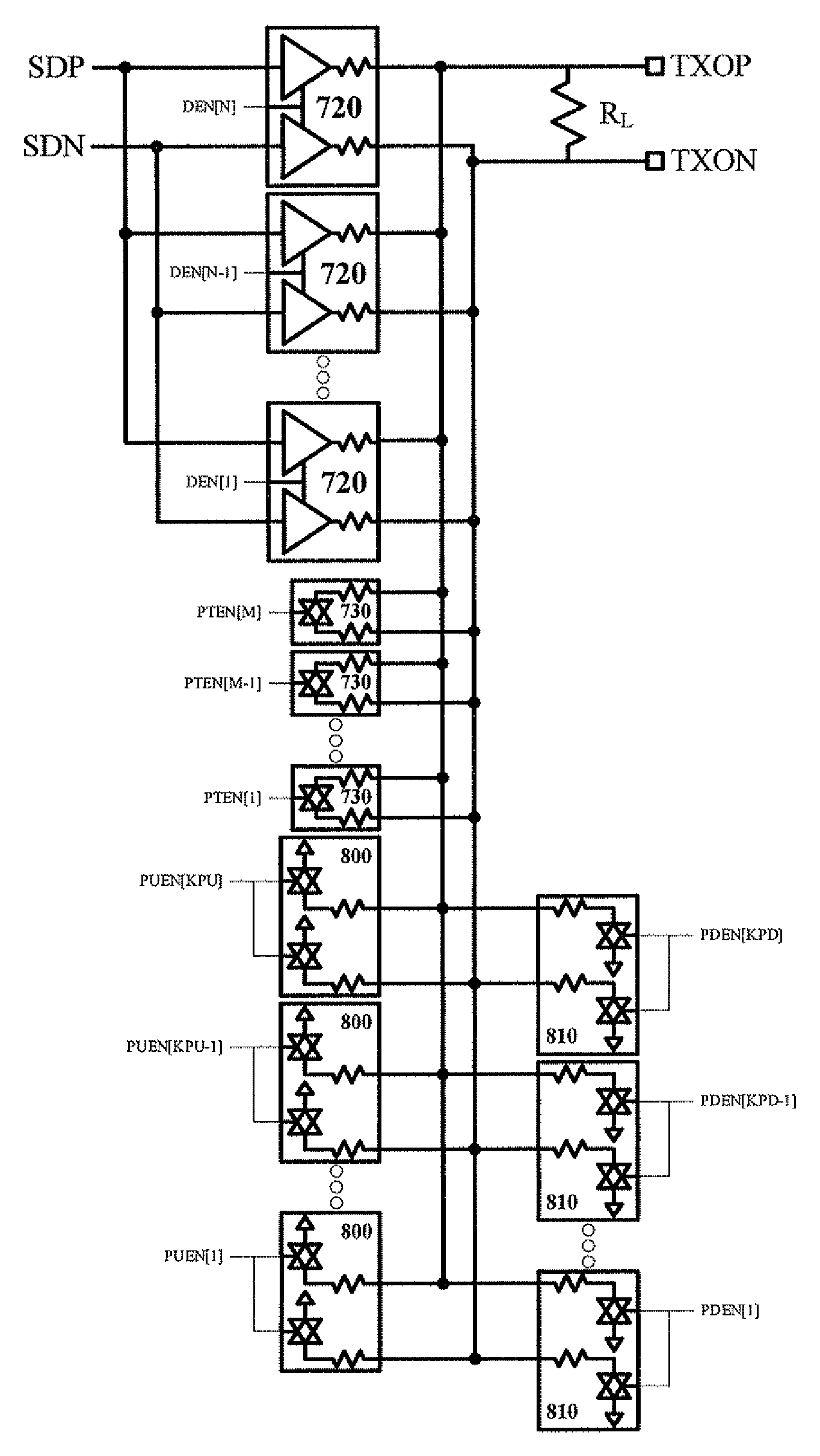
[0072]In a first embodiment, a configurable VM transmitter can be constructed from combinations of two basic “unit cells” (also referred to simply as “cells”), a drive unit cell 720 shown in FIG. 7B and a parallel termination unit cell 730 shown in FIG. 7C. An exemplary drive cell 720 includes two drive cell elements 700a,b (each shown in FIG. 7A as a cell element 700), each drive cell element operative to receive a common enable / disable control signal EN / ENB 726, and two resistors R* 728a,b, interconnected with an output port 724 as shown in FIG. 7B. An exemplary parallel termination cell 730 (FIG. 7C) includes two resistors 736a,b and a transmission gate 738 interconnected with an output port 732 as well as an enable / disable control port (EN) 734 connected to transmission gate 738. The enable / disable control port and the transmission gate form an “enable / disable function”.

[0073]Each drive cell element 700 implements a tri-state buffer with an input port (IN) 701, an output port (O...

second embodiment

[0110]If the number of enabled drive cells is denoted D, the number of enabled parallel termination cells is denoted PT, and the number of enabled pull-up and pull-down cells is denoted PU and PD, respectively, then the established resistive paths between VDD, VSS, and TXOP and TXON, loaded by a resistor RL when logic 1 is being transmitted is illustrated in FIG. 9. The differential and common-mode output characteristics of the second embodiment configuration are given in Equation 7. The derivative of VCM with respect to PU and PD is given in Equation 8.

[0111]ROdiff=2⁢RD+PT+PU+PD⁢⁢VOdiff=2·VDD·DD+PT+PU+PD·RLRL+ROdiff⁢⁢RCM=R2⁢(D+PU+PD)⁢⁢VCM=VDD2·D+2⁢PUD+PU+PD(7)∂VCM∂PU=-∂VCM∂PD=VDD2·D+2⁢PD(D+PU+PD)2(8)

The operating methodologies and the characteristics for this modified transmitter architecture are similar to those outlined for the basic architecture of the first embodiment (see Table 3), with the parameter PT replaced by PT+PU+PD.

[0112]It is apparent from Equations 7 and 8 that VCM ...

third embodiment

[0127]Note also that the description of this third embodiment thus far has specifically referred to the implementation of post-cursor pre-emphasis, whereas in the general case any form of pre-emphasis could be implemented.

[0128]Finally, it should be appreciated that the addition of pull-up and pull-down functions to the configurable VM transmitter of this third embodiment is straightforward through the addition of pull-up and pull-down cells to the VM transmitter of FIG. 10.

[0129]Operationally, similar to the first embodiment with pre-emphasis, the number of enabled drive cells (used for regular drive) is DREG, the number of enabled pre-emphasis unit cells (to drive emphasized bits, or serve as parallel termination for non-emphasized bits) is PRE, and the number of enabled parallel termination cells is PT. In this case, with reference to the expression for VOdiff in Table 3 for the configurable VM transmitter with basic pre-emphasis, for emphasized bits, parameter D is replaced by D...


PUM


Abstract

Configurable voltage mode transmitter architectures are based on combinations of drive cells and parallel termination cells connected in parallel across an external load to provide configurable output characteristics. Each drive cell and parallel termination can be individually enabled, various configurations of enabled cells providing the output characteristics configurability. In some embodiments, dedicated or configured pre-emphasis drive cells with individual enablement capability are added. In some embodiments, pull-down and pull-up cells with individual enablement capability are added to provide additional configurability options. When present, the pre-emphasis, pull-down and pull-up cells are connected in parallel across the external load to provide pre-emphasis features to the output.

Description

CROSS REFERENCE TO RELATED APPLICATIONS[0001]The present invention claims priority from U.S. Provisional Patent Application No. 60 / 809,904 filed 26 May 2006, which is incorporated herein by reference in its entirety.FIELD OF THE INVENTION[0002]The present invention relates in general to transmitters used to drive signals off-chip and in particular to voltage mode transmitters.BACKGROUND OF THE INVENTIONTransmitter Architectures[0003]A transmitter is an output driver of an integrated circuit for the general purpose of transmitting signals originating from one device to other devices in an electronic system. In modern electronic systems, data transmission typically occurs at high data rates (>100 Mbps) over transmission-line type signal lines with transmitter and receiver end-terminations.[0004]For long signal lines, it is common to employ differential signal encoding to mitigate the effects of signal degradation (e.g. noise), in addition to pre-emphasis techniques, the latter prov...

Claims


Application Information

Patent Timeline
Patent Type & Authority Patents(United States)
IPC IPC(8): H03K17/16H03K19/003
CPCH03K19/017581H03K19/018557
Inventor VENDITTI, MICHAEL BENLYE, WILLIAM MICHAEL
Owner PMC-SIERRA
Why Eureka
Try Eureka