Power semiconductor module

a technology of semiconductor modules and semiconductor substrates, applied in semiconductor devices, semiconductor/solid-state device details, electrical apparatus, etc., can solve the problems of affecting the operation of the device, the electrodes on both sides of the drive circuit substrate, and the prone to partial discharge, etc., to achieve the effect of prolonging the operating li

Active Publication Date: 2009-04-07
MITSUBISHI ELECTRIC CORP
View PDF12 Cites 6 Cited by
  • Summary
  • Abstract
  • Description
  • Claims
  • Application Information

AI Technical Summary

Benefits of technology

[0006]The present invention has been devised to solve the above problem. It is, therefore, an object of the present invention to provide a power semiconductor module in which partial discharge is reduced to achieve a longer operating life.
[0008]The present invention allows reduction of partial discharge within a power semiconductor module, resulting in an extended operating life.

Problems solved by technology

However, when the power semiconductor module is used at a high voltage, a partial discharge may occur from a floating potential portion within the module, resulting in insulation failure.
It has been found that drive circuit substrates having electrodes on both sides and having a complicated shape are especially susceptible to partial discharge.

Method used


Image

  • Power semiconductor module
  • Power semiconductor module
  • Power semiconductor module

Examples


first embodiment

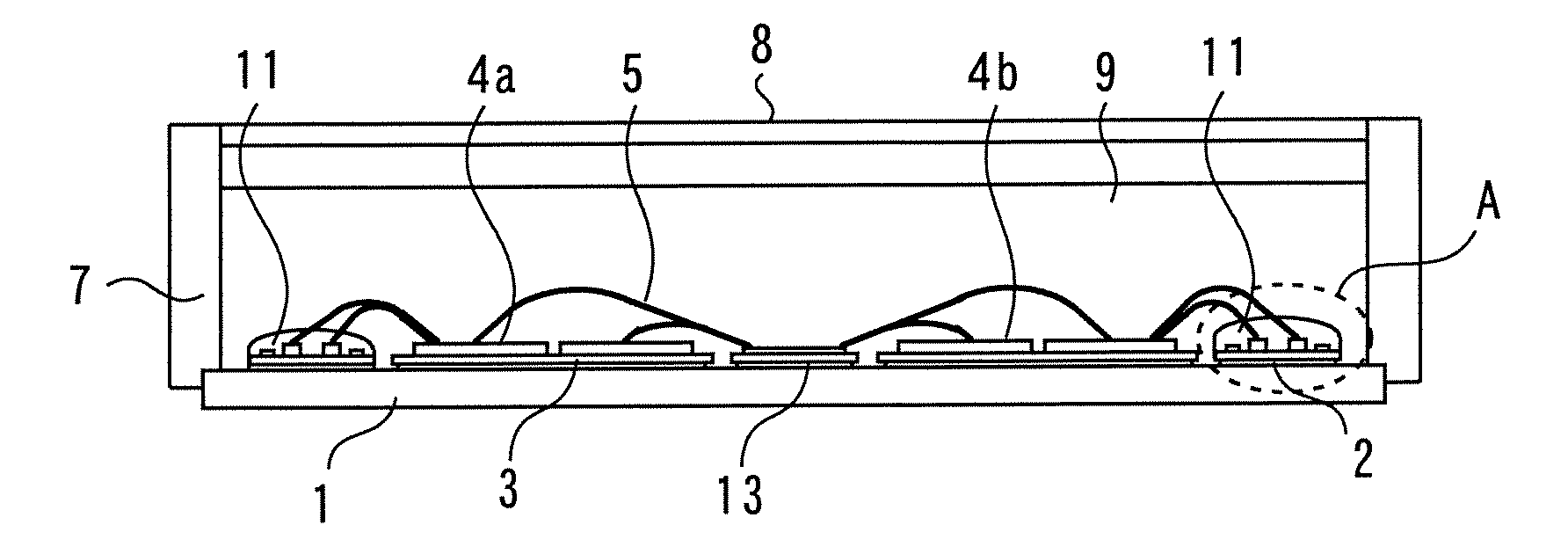
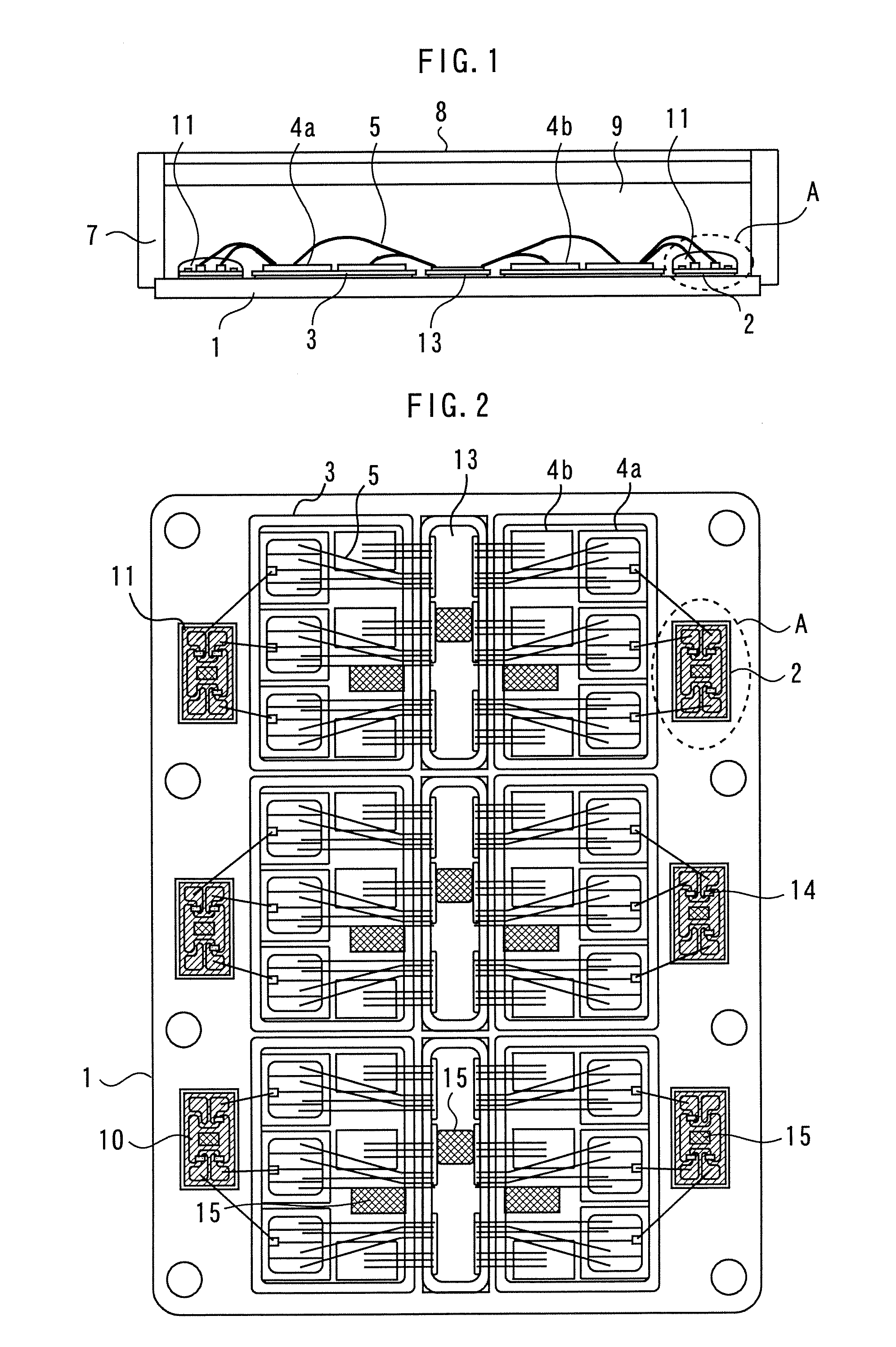
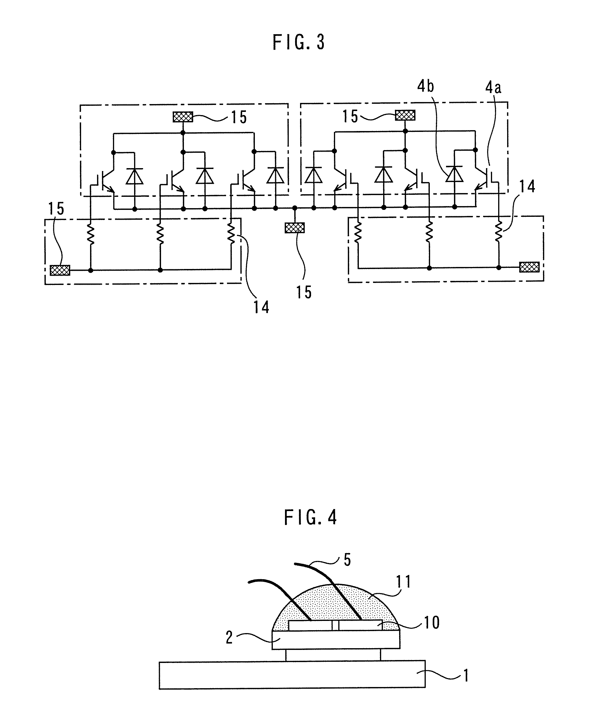
[0017]FIG. 1 is a cross-sectional view of a power semiconductor module according to a first embodiment of the present invention, and FIG. 2 is a top view of the module. This power semiconductor module comprises a plurality of circuit blocks each including a plurality of parallel-connected IGBTs that share common collector, emitter, and gate terminals to achieve high electrical strength and high current operation. For reference, FIG. 3 shows an equivalent circuit of such a circuit block.

[0018]Referring to FIGS. 1 and 2, drive circuit substrates 2 (circuit substrates), power semiconductor circuit substrates 3, and junction circuit substrates 13 are mounted on a metal base plate 1 (a heat sink). Each circuit substrate includes an insulating substrate of a ceramic material, etc. and a conductive (or electrode) pattern 10 of copper or aluminum, etc. formed on both sides of the insulating substrate. Power semiconductor devices (chips) 4, such as insulated gate bipolar transistors (IGBTs) ...

second embodiment

[0022]FIG. 5 is a top view of a drive circuit substrate according to a second embodiment of the present invention. According to the second embodiment, the conductive pattern 10 has round corners. All other components are similar to those described in connection with the first embodiment. This embodiment allows further reduction of partial discharge on the drive circuit substrate, resulting in a longer operating life of the product, as compared to the first embodiment.

third embodiment

[0023]FIG. 6 is a top view of a drive circuit substrate according to a third embodiment of the present invention. According to the third embodiment, the conductive pattern 10 has a round shape and is not covered with a low dielectric constant film 11. All other components are similar to those described in connection with the first embodiment. This embodiment also allows reduction of partial discharge on the drive circuit substrate 2 (which has a complicated shape), resulting in an extended operating life of the product.


PUM


Abstract

A power semiconductor module of the present invention comprises: a heat sink 1; a circuit substrate 2 mounted on the heat sink 1; a conductive pattern 10 provided on the circuit substrate 2; a low dielectric constant film 11 covering the conductive pattern 10; a case 7 provided on the heat sink 1 so as to enclose the circuit substrate 2; and a soft insulator 9 filling the space within the case 7. The low dielectric constant film 11 is preferably formed of silicon rubber, polyimide, or epoxy resin.

Description

BACKGROUND OF THE INVENTION[0001]1. Field of the Invention[0002]The present invention relates to a power semiconductor module in which partial discharge is reduced to achieve a longer operating life.[0003]2. Background Art[0004]A conventional power semiconductor module, such as that proposed in Japanese Laid-Open Patent Publication No. 2002-76197, includes: a heat sink; a circuit substrate(s) mounted on the heat sink; a conductive pattern provided on the circuit substrate; a case provided on the heat sink so as to enclose the circuit substrate; a soft insulator filling the space within the case; and a solid insulator provided on the top surface of the circuit substrate such that it is in contact with the peripheral portion of the conductive pattern. The solid insulator is intended to enhance the insulation resistance and the withstand voltage of the module.[0005]However, when the power semiconductor module is used at a high voltage, a partial discharge may occur from a floating pote...

Claims


Application Information

Patent Timeline
Patent Type & Authority Patents(United States)
IPC IPC(8): H01L23/34
CPCH01L23/5385H01L24/49H01L25/162H01L2924/1305H01L25/072H01L25/18H01L2224/45124H01L2224/48091H01L2224/49H01L2924/01004H01L2924/01013H01L2924/01014H01L2924/01029H01L2924/01033H01L2924/01058H01L2924/01082H01L24/45H01L2224/49175H01L2224/49111H01L2924/13055H01L2924/014H01L2924/01068H01L24/48H01L2924/01006H01L2924/00014H01L2924/00H01L2924/181H01L2224/8592
Inventor KAWAGUCHI, YASUTOHAYASHIDA, YUKIMASA
Owner MITSUBISHI ELECTRIC CORP
Why Eureka
Try Eureka