
Organic electroluminescent device and manufacuring method thereof

a technology of electroluminescent devices and manufacturing methods, which is applied in the direction of solid-state devices, semiconductor devices, corona discharge, etc., can solve the problems of reducing the efficiency and the life-time of the device, the driving voltage of the device, and the device's stability is greatly affected, so as to maintain the stability of the driver voltage and the effect of long operating life and good stability

Inactive Publication Date: 2005-12-15
AU OPTRONICS CORP
View PDF4 Cites 67 Cited by
  • Summary
  • Abstract
  • Description
  • Claims
  • Application Information

AI Technical Summary

Benefits of technology

[0008] It is therefore an object of the invention to provide an organic electroluminescent device and a manufacturing method thereof. The organic electroluminescent device of the present invention can maintain the stability of a driver voltage with a long period and have good stability and long operating life.
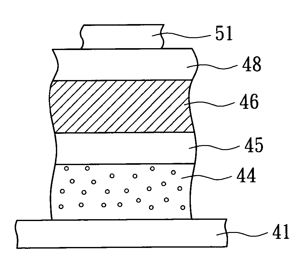
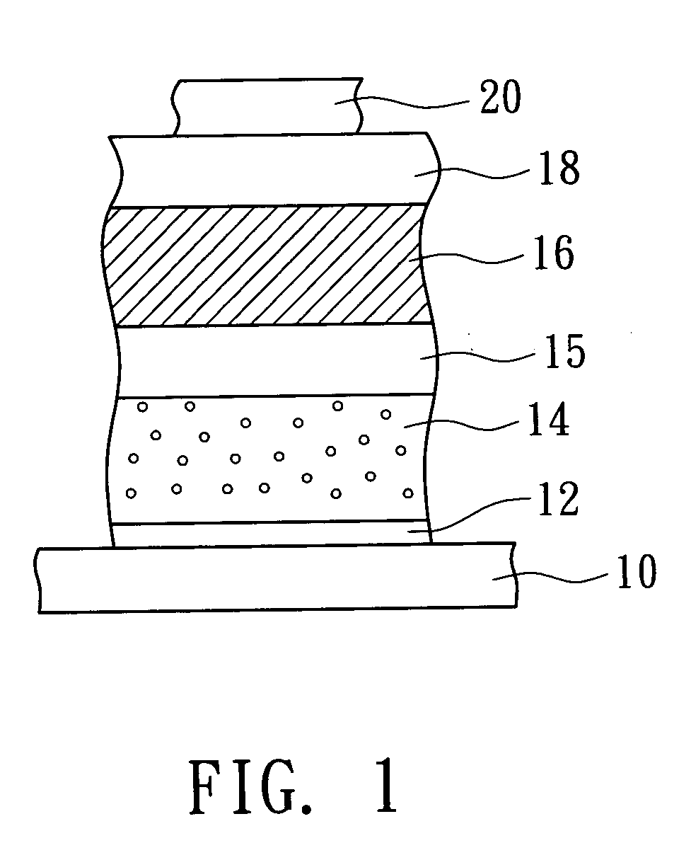
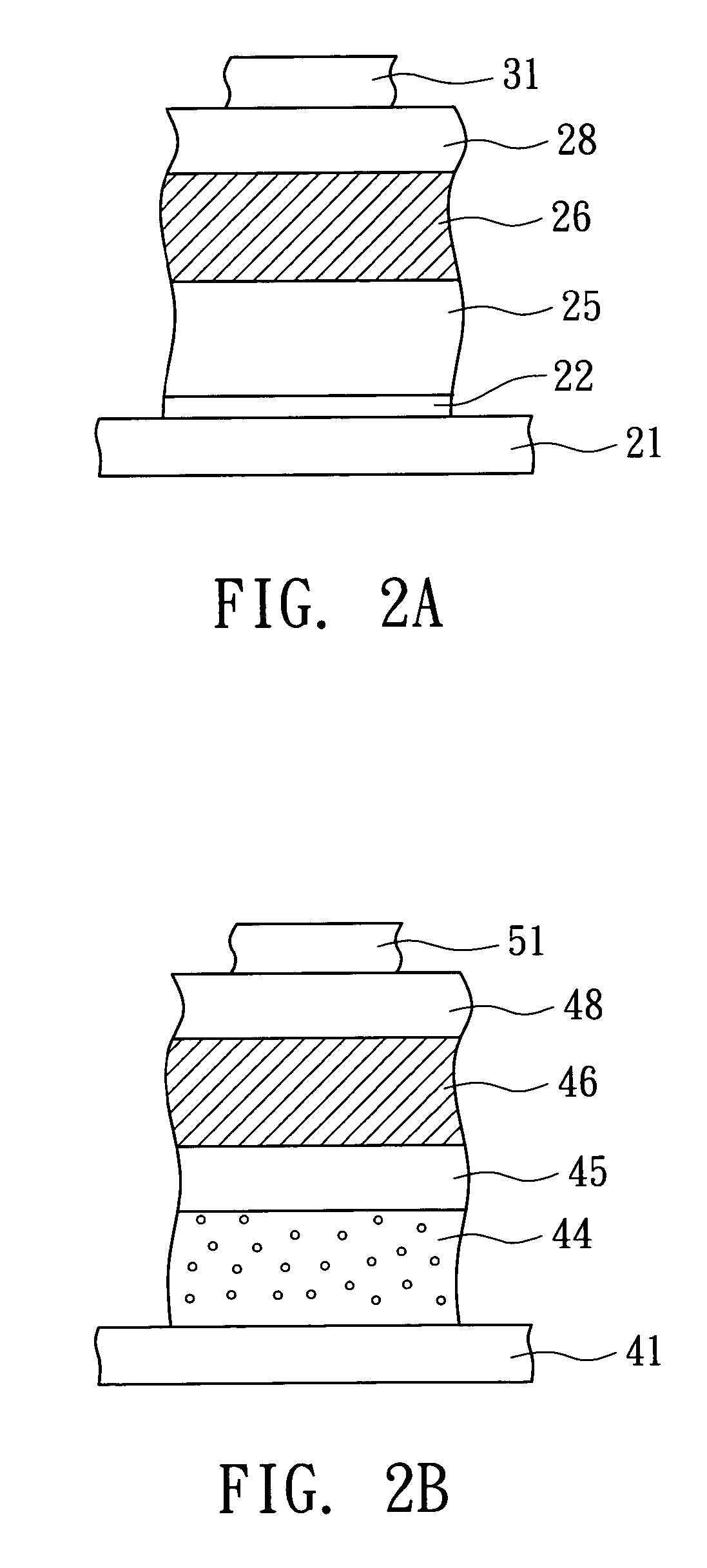
[0010] Also, the invention achieves the above-identified object by providing a manufacturing method of an organic electroluminescent device, comprising the steps of: providing a substrate and forming an anode on the substrate; forming a hole injection layer on the anode; forming a first hole transport layer on the hole injection layer, and the first hole transport layer is doped with a P-type dopant; forming a second hole transport layer on the first hole transport layer; forming a light emitting layer on the second hole transport layer; forming an electron transport layer on the light emitting layer; and forming a cathode on the electron transport layer. According to the invention, the hole injection layer and the first hole transport layer provide the function of increasing the stability of the organic electroluminescent device.

Problems solved by technology

Mobility of holes is greater than that of electrons in the OLED; however, electric charges are accumulated inside the device by such electric unbalance so that the stability of the device is greatly affected.
However, increasing the thickness of the hole transport layer increases driving voltage of the device and decreases the efficiency and the life-time of the device.

Method used


Image

  • Organic electroluminescent device and manufacuring method thereof
  • Organic electroluminescent device and manufacuring method thereof
  • Organic electroluminescent device and manufacuring method thereof

Examples


embodiment

Preferred Embodiment

[0039] Referring to FIG. 1, it is a schematic view of an organic electroluminescent device according to the preferred embodiment of the present invention. An indium tin oxide (ITO) glass substrate is formed by oxygen plasma (O2 plasma) and an anode 10 is formed. Next, a carbon fluorine (CFx) compound thin film is formed on the anode 10 by plasma deposition as a hole injection layer 12. Then, a NPB with the thickness of 150 nm and doped with 2.0% TF-TCNQ, is evaporated on the hole injection layer 12 as a first hole transport layer 14. Next, a second hole transport layer 15 with the thickness of about 100 to 500 Å is formed on the first hole transport layer 14 by evaporating a NPB with the thickness of 20 nm and doping with 2.0% TF-TCNQ. Then, an organic light emitting layer 16, consisting of Alq3, NPB and C545T, is formed on the hole transport layer 15. The composition ratio of material in the organic light emitting layer 16 is [Alq3:NPB]: C545T=[0.5:0.5]:1%., and...


PUM


Abstract

An organic electroluminescent device comprises an anode, a hole injection layer as CFx formed on the anode, a first hole transport layer formed on the hole injection layer and the first hole transport layer doped with a P-type dopant, a second hole transport layer formed on the first hole transport layer, a light emitting layer formed on the second hole transport layer, an electron transport layer formed on the light emitting layer, and a cathode formed on the electron transport layer. According to the structure of the organic electroluminescent device disclosed in the present invention, the hole injection layer and the first hole transport layer provide the function of increasing the efficiency of the hole injection so as to improve the operating life and stability of the device.

Description

[0001] This application claims the priority benefit of Taiwan Patent application Serial No. 93116946, filed Jun. 11, 2004, the subject matter of which is incorporated herein by reference. BACKGROUND OF THE INVENTION [0002] 1. Field of the Invention [0003] The invention relates in general to an electroluminescent device and manufacturing method thereof, and more particularly to an organic electroluminescent device and manufacturing method thereof. [0004] 2. Description of the Related Art [0005] Organic electroluminescent devices, such as organic light-emitting diodes (OLEDs), have been popularly applied to various flat displays because such advantages of self-emissive, very thin form factor, high luminance, high luminous efficiency, high contrast, fast response time, wide viewing angle, low power consumption, wide temperature operation range, and potential of flexible substrate. [0006] The organic electroluminescent device has a multi-layers structure, and the emissive theory of OLED...

Claims


Application Information

Patent Timeline
Patent Type & Authority Applications(United States)
IPC IPC(8): H01L51/50H01L21/312G03G15/02H01L51/30H01L51/00H01L21/00H01L35/24H01L27/15H01L29/08H10N10/856
CPCH01L21/3127H01L51/0051H01L51/5088H01L51/0081H01L51/5052H01L51/0059H10K85/611H10K85/631H10K85/324H10K50/155H10K50/17H01L21/0212
Inventor IOU, CHUNG-YEH
Owner AU OPTRONICS CORP
Learn More