Semiconductor storage device

a storage device and semiconductor technology, applied in the field of semiconductor storage devices, can solve the problems of no use to the circuit, no utilization of the dc type in the conventional dram, etc., and achieve the effect of increasing only the number of redundant cells within the chip, wide spacing, and efficient layou

Inactive Publication Date: 2009-04-28
LONGITUDE SEMICON S A R L
View PDF3 Cites 7 Cited by
  • Summary
  • Abstract
  • Description
  • Claims
  • Application Information

AI Technical Summary

Benefits of technology

[0009]Therefore, an object of the present invention is to provide a semiconductor storage device that is capable of effectively utilizing dummy cells and enhancing the memory cell density.
[0013]It is preferred in the present invention that the terminal memory mats further comprise third bit lines that are connected to corresponding memory cells in response to activation of the prescribed word lines, wherein the third bit lines are connected to one end of sense amplifiers provided to the first sense amplifier array region. The third bit lines are also preferably interposed between the first and second bit lines. This structure makes it possible to arrange the first sense amplifiers in a distributed fashion, and to create an efficient layout. It is also possible to maintain a relatively wide spacing in the layout of the second sense amplifiers, and to arrange the second sense amplifiers so as to be concentrated on the outside of the terminal memory mats.
[0016]It is preferred in the present invention that the first sense amplifiers be disposed between the third bit lines and the fourth bit lines. This structure makes it possible to arrange the first sense amplifiers in a distributed fashion, and to create an efficient layout. It is also possible to maintain a relatively wide spacing in the layout of the second sense amplifiers, and to arrange the second sense amplifiers so as to be concentrated on the outside of the terminal memory mats.
[0019]It is preferred in the present invention that bit lines extending from the first sense amplifier array regions, and bit lines extending from the second sense amplifier array regions be wired in alternating fashion. It is also preferred that bit lines extending from the first sense amplifier array region on one side, and bit lines extending from the first sense amplifier array region on the opposite side be wired in alternating fashion to the intermediate memory mat that is interposed between the first sense amplifier array regions. This structure makes it possible to arrange the first sense amplifiers in a distributed fashion, and to create an efficient layout. It is also possible to maintain a relatively wide spacing in the layout of the second sense amplifiers, and to arrange the second sense amplifiers so as to be concentrated on the outside of the terminal memory mats.
[0020]It is preferred in the present invention that the twin cell unit comprises a redundant cell. This configuration makes it possible to increase only the number of redundant cells within a chip without reducing the capacity of a normal memory cell. Since a twin cell also has tREF characteristics that are superior to those of a single memory cell, even further enhancement of the tREF characteristics over those of a conventional redundant cell can be anticipated.
[0021]According to the present invention, second sense amplifiers that are connected to dummy bit lines are provided, the second sense amplifiers and two adjacent dummy bit lines are connected according to a folded bit line system, and a twin cell is formed using two memory cells on a pair of dummy bit lines that are connected to the second sense amplifiers. Dummy bit lines can therefore be omitted from the terminal memory mats, thereby enhancing the cell density as well as reducing the chip surface area. Since twin cells and normal memory cells can both be disposed on a single chip, reduced power consumption and enhanced refresh characteristics can be anticipated.

Problems solved by technology

However, this type of dummy cell DC is not utilized at all in the conventional DRAM, and was of no use to the circuit.

Method used


Image

  • Semiconductor storage device
  • Semiconductor storage device
  • Semiconductor storage device

Examples


Embodiment Construction

[0032]Preferred embodiments of the present invention will now be described in detail hereinafter with reference to the accompanying drawings.

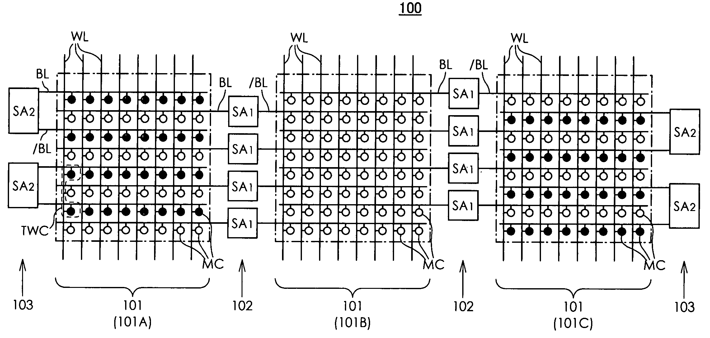
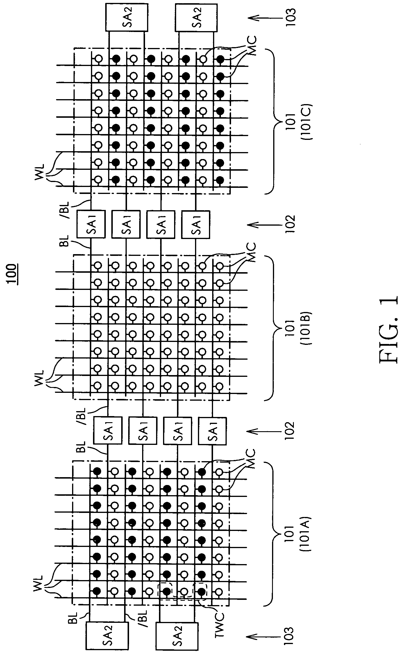
[0033]FIG. 1 is a schematic circuit diagram showing the circuit structure of DRAM according to a preferred embodiment of the present invention.

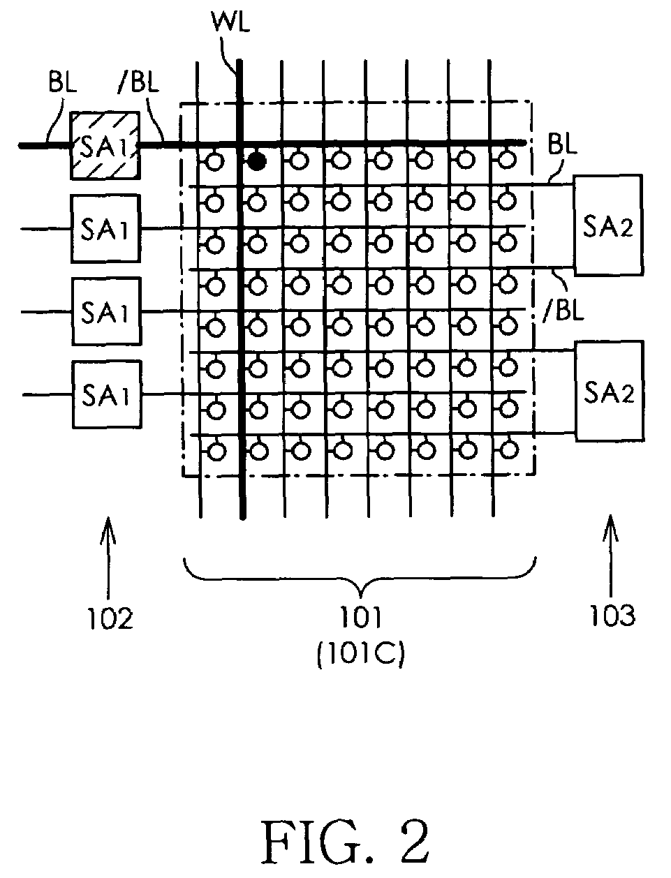
[0034]As shown in FIG. 1, the DRAM 100 is provided with a plurality of memory mats 101 that constitute a region in which a memory cell array is formed, first sense amplifiers SA1 that are provided between adjacent memory mats 101, and second sense amplifiers SA2 that are provided to the outside of the terminal memory mats 101A and 101C. In the present embodiment, the plurality of memory mats 101 and a plurality of sense amplifier array regions 102 and 103 are arranged in alternating fashion. In other words, the plurality of memory mats 101 is broadly classified into an intermediate memory mat 101B that is disposed between the other memory mats that are present on both sides thereof in the row direction (...


PUM


Abstract

A semiconductor storage device that is capable of utilizing dummy cells effectively and enhancing the memory cell density. Every second row of bit lines (second bit lines) in terminal memory mats 101A, 101C is not connected to first sense amplifiers SA1. Second sense amplifiers SA2 are arranged on the outside of the terminal memory mats, and second bit lines are connected according to a folded bit line system to the second sense amplifiers SA2. Two memory cells provided at the points where a word line WL intersects with a pair of bit lines BL, / BL connected to the second sense amplifiers SA2 constitute a twin cell unit TWC for storing a single bit of data in complementary fashion.

Description

TECHNICAL FIELD[0001]The present invention relates to a semiconductor storage device, and particularly relates to DRAM (Dynamic Random Access Memory) or another semiconductor storage device that uses an open bit line system as the system by which a sense amplifier is connected to a bit line pair.BACKGROUND OF THE INVENTION[0002]System by which a sense amplifier is connected to a bit line pair in DRAM, which is a type of semiconductor storage device, include an open bit line system and a folded bit line system (see Japanese Laid-Open Patent Application No. 2003-273245). In an open bit line system, two bit lines that are connected to a single sense amplifier are wired in opposite directions from each other on either side of the sense amplifier. In a folded bit line system, two bit lines that are connected to a single sense amplifier are turned back at the sense amplifier and wired in the same direction.[0003]FIG. 6 is a circuit diagram showing the basic structure of a folded bit line ...

Claims


Application Information

Patent Timeline
Patent Type & Authority Patents(United States)
IPC IPC(8): G11C5/06
CPCG11C5/025G11C7/14G11C7/18G11C11/4097G11C11/4099G11C2211/4013
Inventor KAWAKITA, KEIZOTANAKA, YOSHINORI
Owner LONGITUDE SEMICON S A R L
Why Eureka
Try Eureka