Protection circuit for electro static discharge

a protection circuit and electrostatic discharge technology, applied in the direction of emergency protective arrangements for limiting excess voltage/current, emergency protective arrangements for limiting excess voltage, etc., can solve the problems of abnormal operation of electronic devices or systems, damage to devices and computer systems, and damage to electronic devices or systems by electrical overstress, so as to reduce the occupied area of a single fet component and reduce the equivalent resistance between drain and source

Active Publication Date: 2009-05-12
MEDIATEK INC
View PDF5 Cites 11 Cited by
  • Summary
  • Abstract
  • Description
  • Claims
  • Application Information

AI Technical Summary

Benefits of technology

[0018]A main objective of the present invention is to provide an ESD protection circuit, which employs a FET component having no silicide block. As ESD occurs, an ESD clamp circuit of the ESD protection circuit turns on the FET component to provide an ESD grounding path for draining off the ESD current so as to prevent the internal circuit from damage. The portion of the present invention different from the prior art is that the ESD protection circuit complied with the present invention employs a FET component having no silicide block so that the equivalent resistance between the drain and source can be reduced. Hence, the ESD protection circuit of the present has an equivalent input resistance and capacitance that is suitable for high-frequency input signals or current input signals. Meanwhile, it also can reduce the occupied area of a single FET component. Besides, its ESD resisting ability for HBM or MM is the same as that of the prior art.

Problems solved by technology

In accordance with the prior art, it is well known that ESD is a main factor to cause electronic devices or systems to be damaged by electrical overstress (EOS).
ESD may make semiconductor devices and computer systems be damaged permanently, hence it can influence functions of integrated circuits (IC) and make the electronic devices operate abnormally.
In most situations, ESD is induced artificially, but it is still hard to avoid this effect.
In some circumstances, due to contacting the electronic devices with human bodies, instruments and store equipments unknowingly, it may form a path of ESD and make the electronic devices or systems be damaged unexpectedly.
However, there is still a limit.
When the components operate at the second breakdown region due to the additional EOS current or voltage, they will be damaged permanently.
However, as the deep sub-micron techniques became the main stream of the market, the ESD of the charge device model (CDM) can cause the damage of gate oxide very easily when the thickness of the gate oxide is only 50A made by 0.25 micro manufacturing processes.
Even if the ESD protection circuit is already applied to the gate of the input end, in most situations, it still cannot be turned on timely to drain off the immediately generated ESD current of CDM.
It has large RC delay time for the input signal and is not suitable for applications with high-frequency signals or current input signals.
Since the stray resistances are very small, as the ESD occurs, the ESD current is easily passed to the LDD structure of the MOS components to damage them.
Even if the MOS component with large width / length (W / L) ratio is used as output stage, the ESD resisting ability still can't be improved.
Further, in the viewpoint of input end, the increase of resistance would increase the RC delay time of the input signal.
Hence, this kind of components is not suitable for the inputs with high-frequency signal or current signals.
With the silicide blocks, the ESD resisting ability can be improved certainly, but the increased equivalent input resistance would restrict the application of this kind of component in high-frequency field.

Method used


Image

  • Protection circuit for electro static discharge
  • Protection circuit for electro static discharge
  • Protection circuit for electro static discharge

Examples


Embodiment Construction

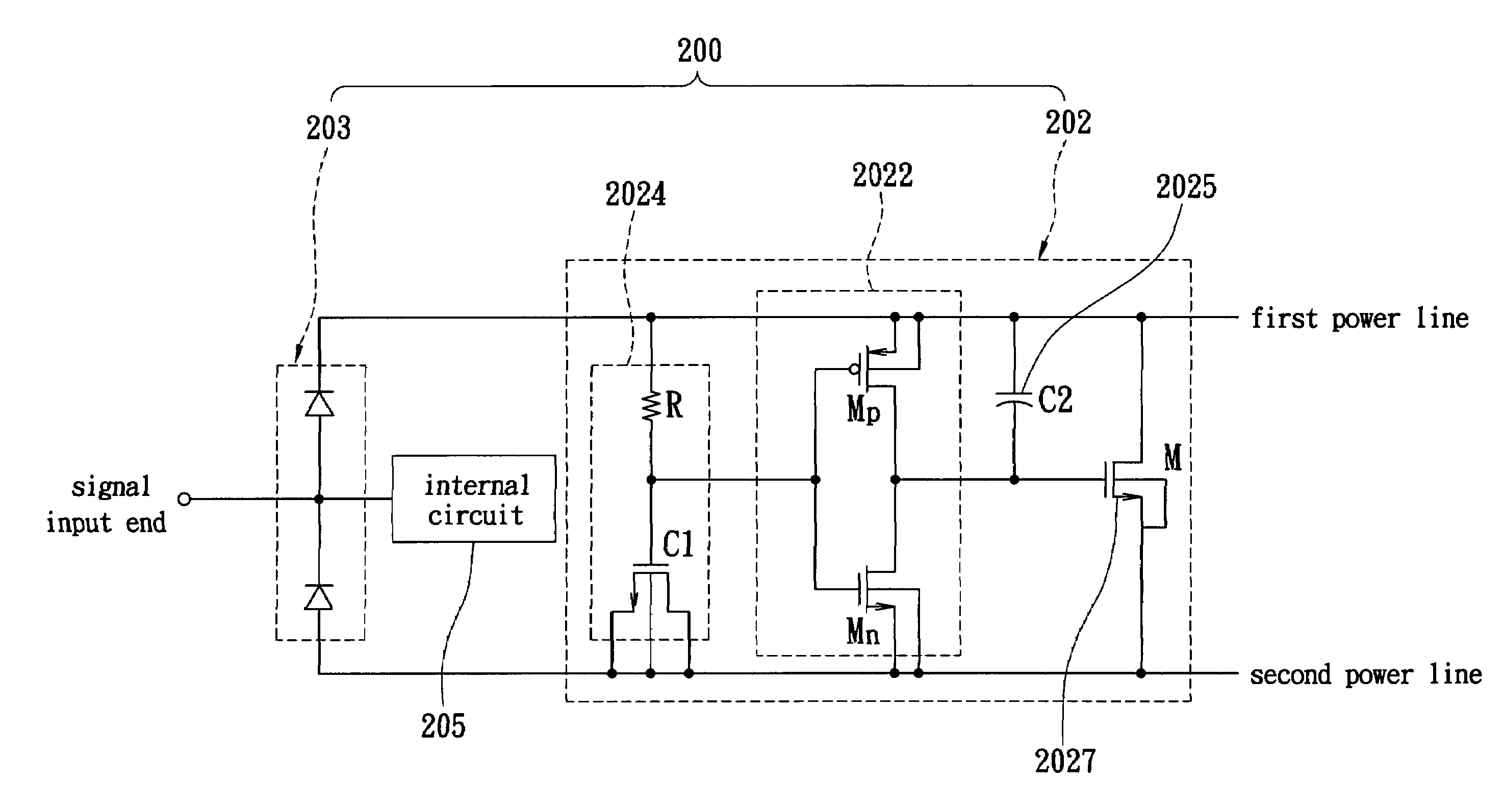
[0028]Please refer to FIG. 5, which shows a schematic diagram of an ESD protection circuit complied with the present invention. The ESD protection circuit has an ESD clamp circuit and at least a pair of p-n junction diodes 203 to prevent the internal circuit 205 from damaged by the ESD (mainly in HBM or MM) induced at the signal input end.

[0029]The ESD clamp circuit 202 includes a CMOS inverter (Mp and Mn) 2022, a RC retarder 2024 (the capacitor C1 is carried out by using a MOS component), a coupling capacitor 2025 (C2) and a FET 2027 (M). Therein, the coupling capacitor C2 is coupled to the FET M. Meanwhile, the drain of the FET M has no silicide block disposed thereon (as shown in FIG. 3a). In the conventional ESD protection circuit, in order to increase the resistance between the drain and source of a FET to restrict the ESD current, the FET must have the silicide block (as shown in FIG. 3b). The ESD protection circuit complied with the present invention has no silicide block and...


PUM


Abstract

An electro static discharge (ESD) protection circuit employing a field-effect transistor (FET) having no silicide block disposed thereon. It is connected with an internal circuit so as to prevent the internal circuit from the influence of an ESD event, wherein the internal circuit has at least a signal input end. The ESD protection circuit includes: an ESD clamp circuit for providing an ESD grounding path as an ESD occurs; and at least a pair of p-n junction diodes. The p-n junction diodes are stacked so that one of the p-n junction diodes has a n-type end coupled to the signal input end and the other one has a p-type end coupled to the signal input end as well. The ESD clamp circuit has at least a FET, whose drain has no silicide block disposed thereon.

Description

[0001]This Nonprovisional application claims priority under 35 U.S.C. § 119(a) on patent application No(s). 092119457 filed in TAIWAN on Jul. 16, 2003, the entire contents of which are hereby incorporated by reference.FIELD OF THE INVENTION[0002]The present invention is directed to a protection circuit for electro static discharge (ESD), and more particularly, to a protection circuit employing a metal-oxide semiconductor field-effect transistor (MOSFET) having no silicide block disposed on its drain.BACKGROUND OF THE INVENTION[0003]In accordance with the prior art, it is well known that ESD is a main factor to cause electronic devices or systems to be damaged by electrical overstress (EOS). ESD may make semiconductor devices and computer systems be damaged permanently, hence it can influence functions of integrated circuits (IC) and make the electronic devices operate abnormally. In most situations, ESD is induced artificially, but it is still hard to avoid this effect. The reason i...

Claims


Application Information

Patent Timeline
Patent Type & Authority Patents(United States)
IPC IPC(8): H02H9/00H01L23/60H01L27/02
CPCH01L27/0255H01L27/0285H01L2924/0002H01L2924/00
Inventor CHENG, TAOLIAO, HSUEH-KUN
Owner MEDIATEK INC
Why Eureka
Try Eureka