Method of manufacturing wiring substrate to which semiconductor chip is mounted

a manufacturing method and semiconductor chip technology, applied in the direction of printed capacitor incorporation, conductive pattern formation, printed electric component incorporation, etc., can solve the problems of limiting the manufacturing of a thinner/smaller wiring substrate for such decoupling capacitors and the limit of manufacturing a thinner/smaller wiring substra

Active Publication Date: 2009-05-26
SHINKO ELECTRIC IND CO LTD
View PDF12 Cites 28 Cited by
  • Summary
  • Abstract
  • Description
  • Claims
  • Application Information

AI Technical Summary

Problems solved by technology

However, in the related cases of mounting the decoupling capacitor to the wiring substrate, there is a limit to manufacturing a thinner decoupling capacitor and a limit to manufacturing a thinner / smaller wiring substrate for such decoupling capacitor.

Method used


Image

  • Method of manufacturing wiring substrate to which semiconductor chip is mounted
  • Method of manufacturing wiring substrate to which semiconductor chip is mounted
  • Method of manufacturing wiring substrate to which semiconductor chip is mounted

Examples


Embodiment Construction

[0032]In the following, embodiments of the present invention are described with reference to the accompanying drawings.

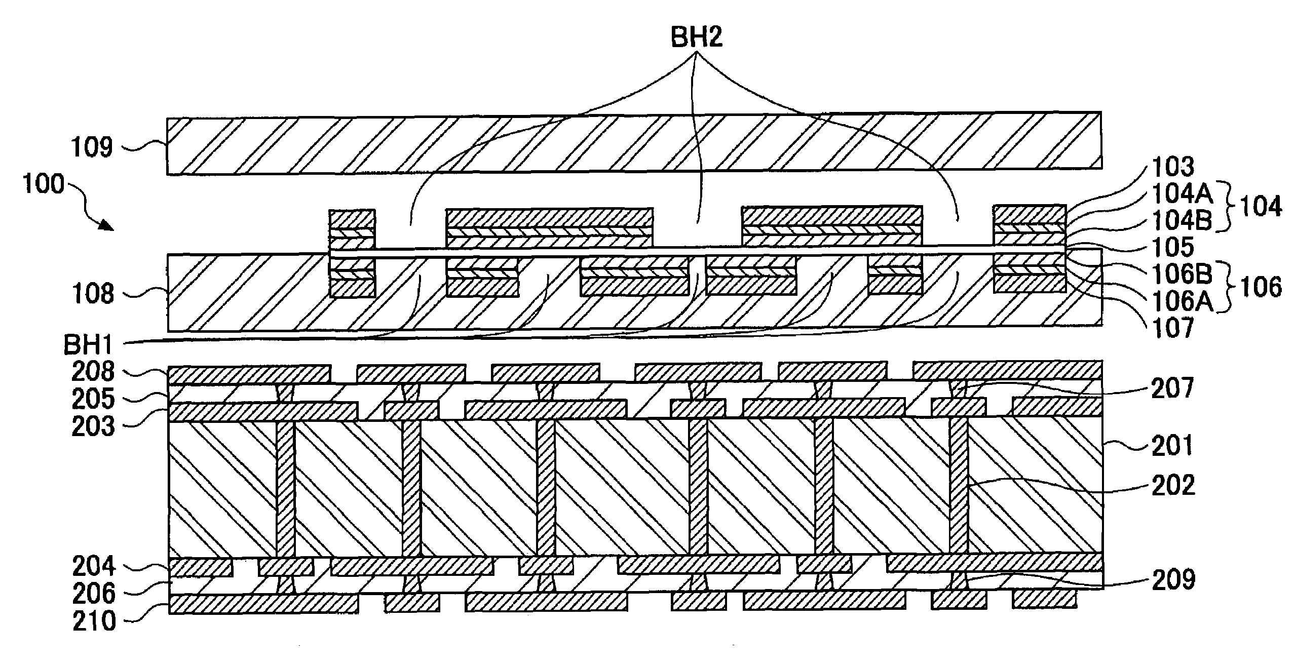
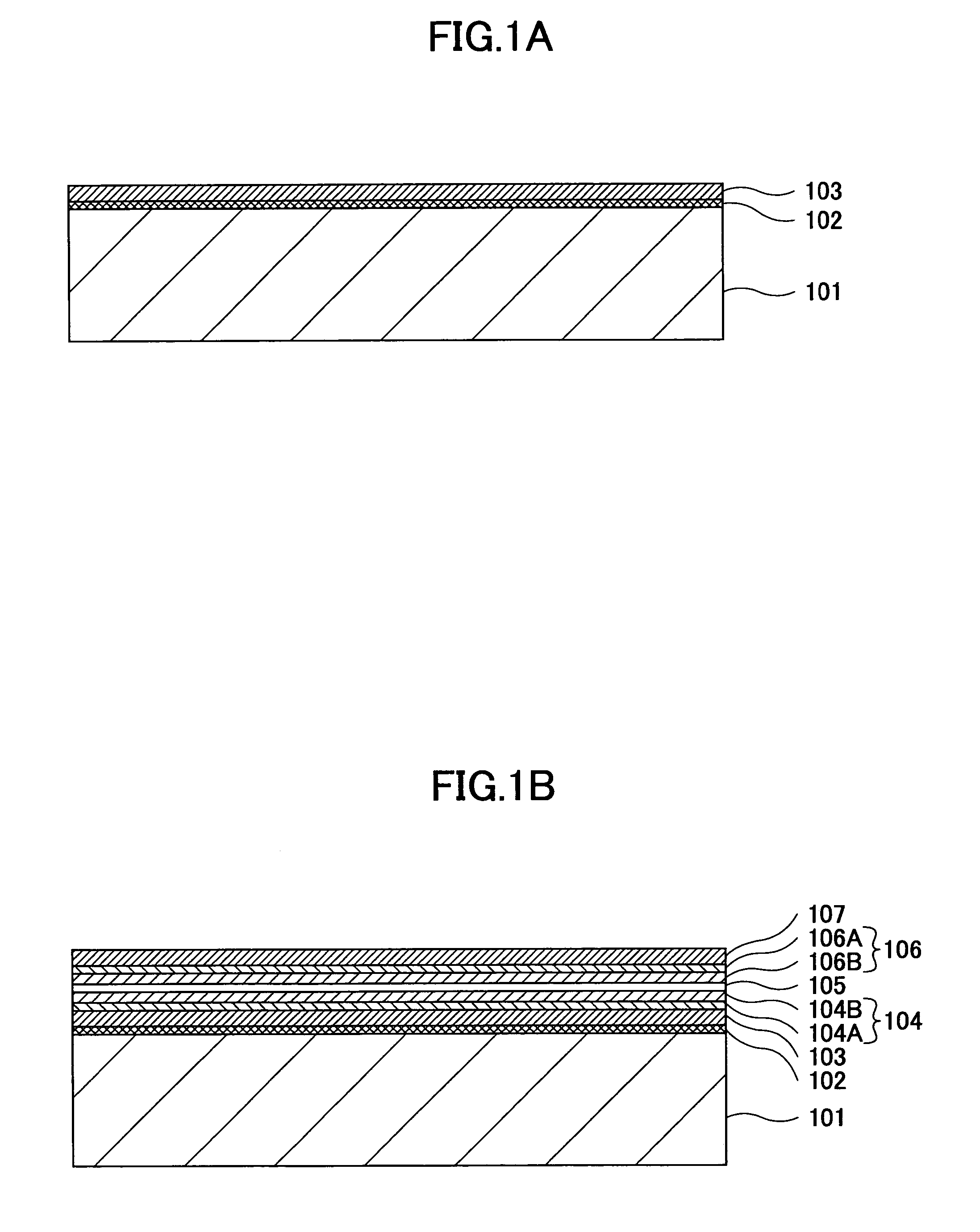
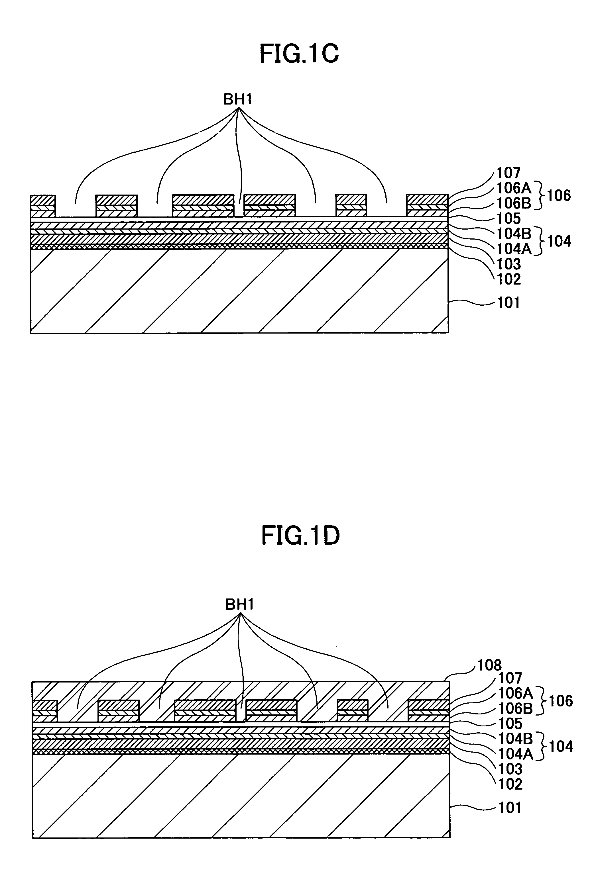
[0033]A method of forming a capacitor 100 according to an embodiment of the present invention is described with reference to FIGS. 1A-1F.

[0034]In FIG. 1A, a base 101 includes a peeling layer 102 formed thereon. The base 101 includes, for example, at least one of Si, glass (silica glass, borosilicate glass) and metal material. In this example, the base 101 has a thickness of approximately 500 μm to 1000 μm. In this example, the peeling layer 102 has a thickness of approximately 500 nm to 1000 nm.

[0035]The capacitor 100 (See FIG. 1F) according to an embodiment of the present invention includes plural layers which are to be formed on the peeling layer 102 in a subsequent step (described below). Furthermore, the base 101 is peeled apart from the plural layers of the capacitor 100 in another subsequent step so as to reduce the thickness of the capacitor 100. The peeling ...


PUM

PropertyMeasurementUnit
thicknessaaaaaaaaaa
thicknessaaaaaaaaaa
thicknessaaaaaaaaaa

Abstract

The present invention discloses a method of manufacturing a wiring substrate to which a semiconductor chip mounted. The method includes the steps of forming a base, forming a peeling layer on the base, forming a capacitor having a plurality of layers on the peeling layer, and forming a wiring part in the capacitor for connecting the capacitor to the semiconductor chip.

Description

BACKGROUND OF THE INVENTION[0001]1. Field of the Invention[0002]The present invention generally relates to a method of manufacturing a wiring substrate, having a semiconductor chip decoupling capacitor, to which a semiconductor chip is mounted.[0003]2. Description of the Related Art[0004]In recent years and continuing, there is a trend for forming smaller and thinner semiconductor devices (e.g. semiconductor chips). Along with this trend, there is a growing demand for forming smaller and thinner decoupling capacitors (also referred to as “decoupling condenser” and “bypass condenser”) used for stabilizing operations by controlling changes of electric voltage of a semiconductor chip, for example.[0005]Furthermore, since the operating frequency of semiconductor chips is expected to be increased for improving the operating speed of semiconductor chips, the decoupling capacitor is preferred to be set (positioned) as near as possible to the semiconductor chip so as to reduce the inductanc...

Claims


Application Information

Patent Timeline
Patent Type & Authority Patents(United States)
IPC IPC(8): H05K3/36
CPCH01L21/4857H01L23/49822H01L23/50H01L24/16H05K1/162H01L21/6835Y10T29/49155H01L2221/68345H01L2224/13099H01L2224/16H01L2924/01015H01L2924/01022H01L2924/01029H01L2924/01038H01L2924/0104H01L2924/01042H01L2924/01056H01L2924/01073H01L2924/01078H01L2924/01079H01L2924/01082H01L2924/19041H01L2924/30105H01L2924/30107H01L2924/3011H05K3/025H05K3/4602H05K2201/0179H05K2201/09309H05K2201/09481H05K2201/09518H05K2201/09718H05K2201/10674H05K2203/016H05K2203/061H01L2924/01006H01L2924/01023H01L2924/01033H01L2924/014H01L2224/16235Y10T29/49126Y10T29/49165H01L2924/00014H01L2924/00011H01L2224/0401
Inventor SHIMIZU, NORIYOSHIYAMASAKI, TOMOOOI, KIYOSHIROKUGAWA, AKIO
Owner SHINKO ELECTRIC IND CO LTD
Why Eureka
Try Eureka