Semi-transmissive liquid crystal display panel

a liquid crystal display panel and semi-transmissive technology, applied in non-linear optics, instruments, optics, etc., can solve the problems of poor visibility in poorly-lit rooms, large amount of backlight, time-consuming exposure process, etc., and achieve satisfactory image quality and high contrast

Inactive Publication Date: 2009-05-26
JAPAN DISPLAY WEST
View PDF8 Cites 0 Cited by
  • Summary
  • Abstract
  • Description
  • Claims
  • Application Information

AI Technical Summary

Benefits of technology

[0030]With this structure, the following advantage is obtained. Since the reflecting layer has a notch portion at the edge thereof and a contact hole is formed in a position corresponding to the notch portion, a mask that is used when a photoresist is exposed to light is open toward the transmissive portion or an adjacent reflecting layer at an end thereof that corresponds to the notch portion of the reflecting portion. From this open end of the mask, part of exposure light leaks into an opening of a contact hole portion due to a scattering of light. As a result, even when a photoresist applied to the surface of a coating of reflecting layer forming material becomes thicker inside the opening of the contact hole portion than in an inter-reflecting-layer region at the time of formation of a reflecting layer, exposures of the photoresist in the contact hole portion and the photoresist in the inter-reflecting-layer region can be performed at the same time and in a shorter time period compared to the conventional example, enhancing production efficiency of the semi-transmissive liquid crystal display panel.
[0042]Incidentally, in an MVA semi-transmissive liquid crystal display panel, when no electric field is applied, even when a pixel electrode does not overlap scan and signal lines in a transmissive portion, as seen in a plan view, there is no possibility of light leakage. However, a voltage applied to the scan line varies greatly, affecting the liquid crystal molecules. This may cause disturbance in the alignment of the liquid crystal molecules in the transmissive portion near the scan line, causing leakage of light. By adopting the structure of the present invention, since the electric field produced by the scan line is blocked by the pixel electrode, it does not affect the liquid crystal molecules. This makes it possible to obtain an MVA semi-transmissive liquid crystal display panel that suffers less from light leakage occurring in the transmissive portion, and that offers high contrast and satisfactory image quality.

Problems solved by technology

Disadvantageously, the backlight consumes a large amount of electric power.
The problem here is that this reflective liquid crystal display device uses external light as its light source, and hence suffers from poor visibility in a poorly-lit room, for example.
Now, since, for example, the users of mobile devices typified by mobile phones or the like are limited, there has conventionally not been so much demand to use a liquid crystal display panel having a wide viewing angle in small display portions of such mobile devices.
The problem here is that, since the photoresist applied to the surface of the coating of reflecting layer forming material also fills the opening of the contact hole portion formed in the interlayer film 17, the photoresist to be exposed to light is thicker inside the opening of the contact hole portion than in an inter-reflecting-layer region.
This disadvantageously makes the exposure a time-consuming process.
When liquid crystal display panels are mass-produced, the longer exposure time leads to reduction in production efficiency due to accumulated exposure time.

Method used


Image

  • Semi-transmissive liquid crystal display panel
  • Semi-transmissive liquid crystal display panel
  • Semi-transmissive liquid crystal display panel

Examples


Embodiment Construction

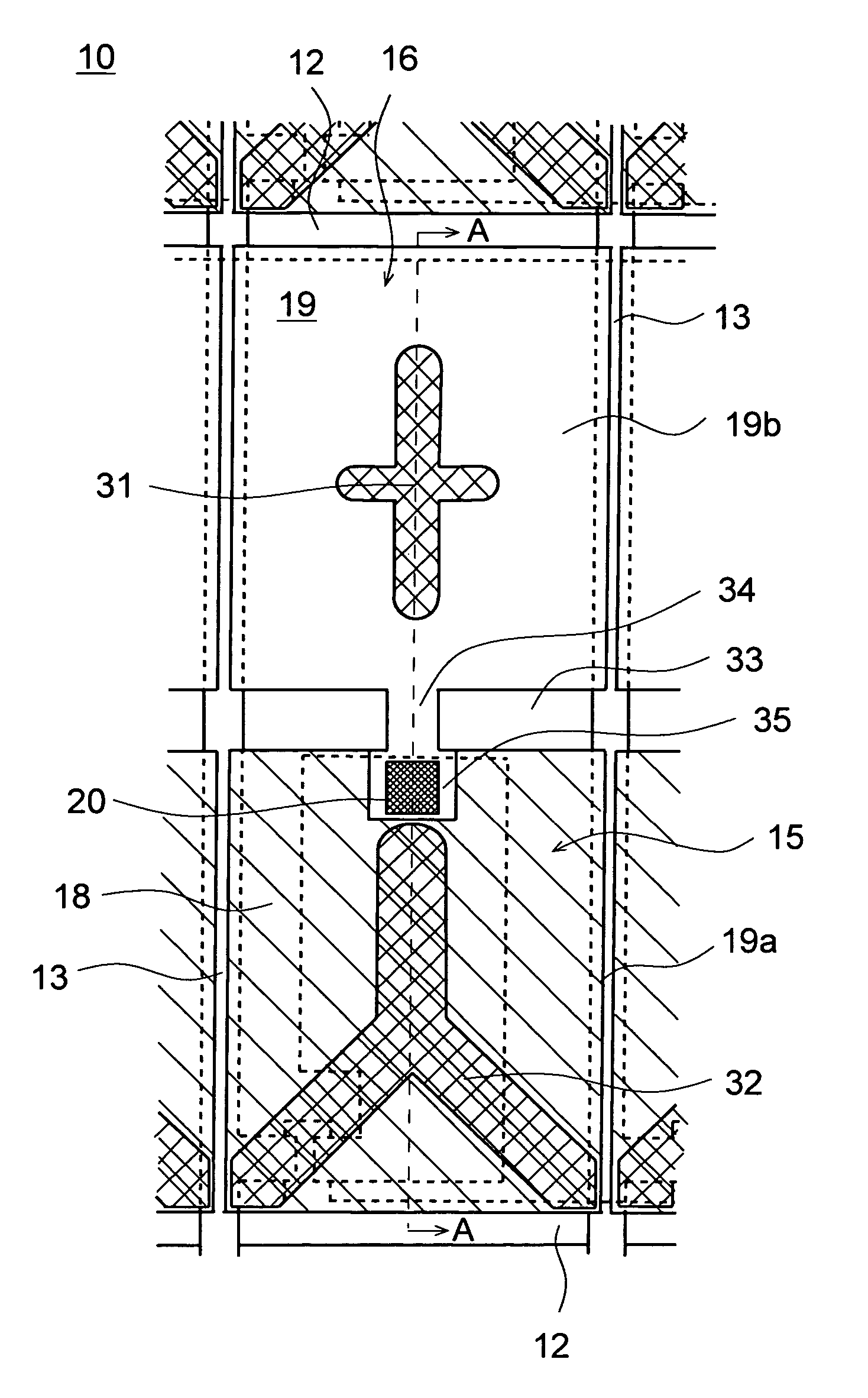
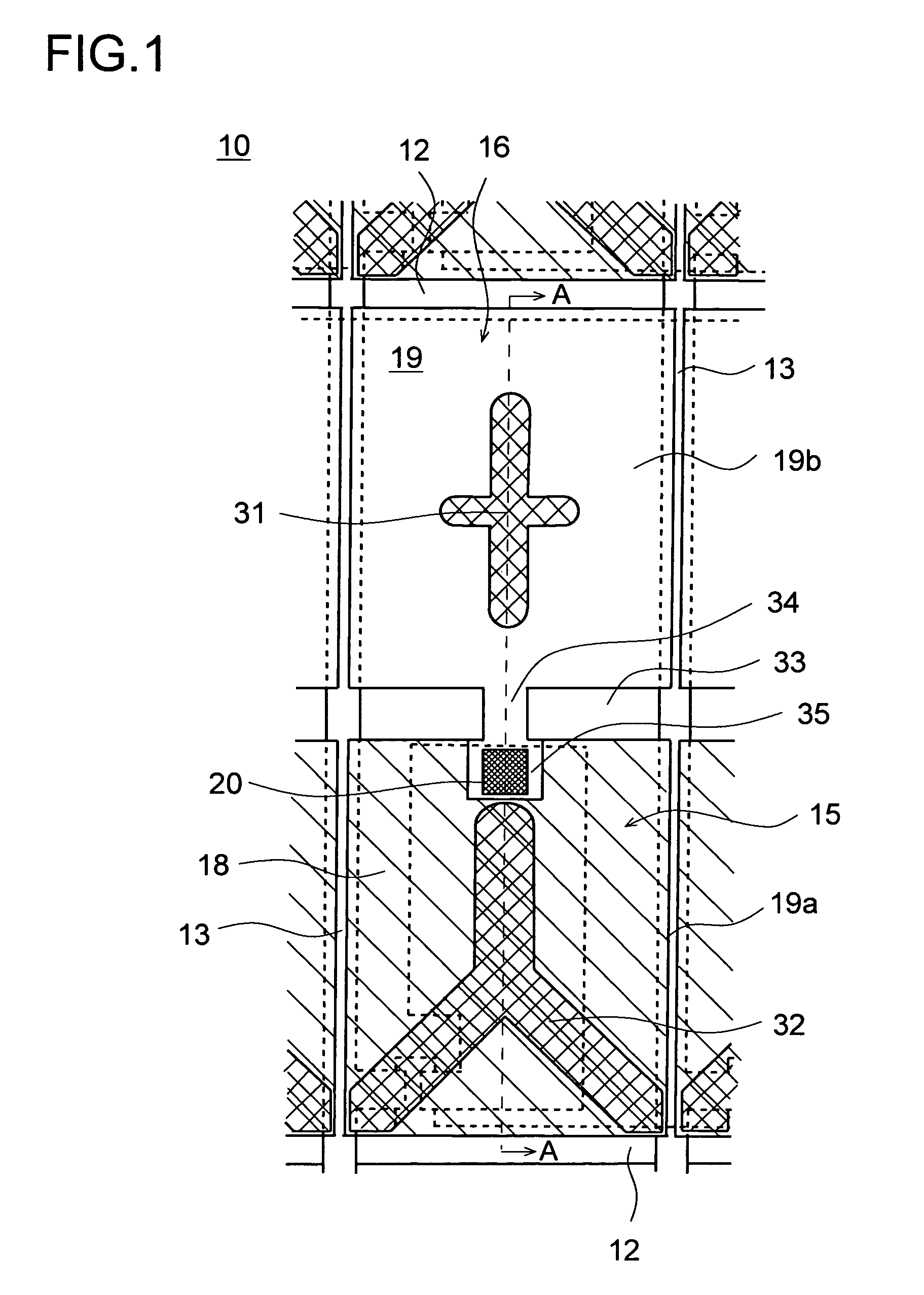
[0053]Hereinafter, embodiments of the present invention will be described specifically with reference to the accompanying drawings. It should be understood, however, that the embodiments presented below are simply intended to give an example of a semi-transmissive liquid crystal display panel that embodies the technical idea of the present invention, and therefore the semi-transmissive liquid crystal display panel specifically described below is not intended to limit in any way the manner in which to carry out the present invention. That is, the present invention finds wide application in the technical fields to which the appended claims are directed.

[0054]An MVA semi-transmissive liquid crystal display panel 10 embodying the present invention will be described with reference to FIGS. 1 to 3. FIG. 1 is a plan view showing one pixel of the MVA semi-transmissive liquid crystal display panel 10, as seen through the second substrate. FIG. 2 is a sectional view taken along line A-A shown...


PUM

PropertyMeasurementUnit
exposure timeaaaaaaaaaa
timeaaaaaaaaaa

Abstract

An semi-transmissive liquid crystal display panel is provided with a first substrate divided into sections by signal lines and scan lines arranged so as to form a matrix, each section having a switching element and a pixel electrode, the pixel electrode having transmissive and reflective portions. Here, at least the reflective portion of the first substrate has an interlayer film formed therein for separating the pixel electrode and the switching element, and a reflecting layer located below the pixel electrode, the reflecting layer has a notch portion at the edge thereof, and the pixel electrode formed in the reflective portion is electrically connected to an electrode of the switching element via a contact hole that is formed through the interlayer film in a part thereof corresponding to the notch portion.

Description

[0001]This application is based on Japanese Patent Application No. 2005-277245 filed on Sep. 26, 2005, the contents of which are hereby incorporated by reference.BACKGROUND OF THE INVENTION[0002]1. Field of the Invention[0003]The present invention relates to a semi-transmissive liquid crystal display panel, and more particularly to a semi-transmissive liquid crystal display panel that can reduce contact hole formation time and thus offer a satisfactory production efficiency.[0004]2. Description of Related Art[0005]In recent years, it has been becoming increasingly popular to use liquid crystal display devices not only in information communication devices but also in commonly used electric devices. A liquid crystal display device itself does not emit light, and hence a transmissive liquid crystal display device provided with a backlight is widely used. Disadvantageously, the backlight consumes a large amount of electric power. It is for this reason that, to reduce the electric power ...

Claims


Application Information

Patent Timeline
Patent Type & Authority Patents(United States)
IPC IPC(8): G02F1/1335
CPCG02F1/133555G02F1/136227G02F1/133707
Inventor YOSHIDA, KOJITANAKA, SHINICHIRO
Owner JAPAN DISPLAY WEST
Why Eureka
Try Eureka