Method for providing mixed stacked structures, with various insulating zones and/or electrically conducting zones vertically localized

Inactive Publication Date: 2009-06-02
COMMISSARIAT A LENERGIE ATOMIQUE ET AUX ENERGIES ALTERNATIVES
View PDF11 Cites 8 Cited by
  • Summary
  • Abstract
  • Description
  • Claims
  • Application Information

AI Technical Summary

Problems solved by technology

This problem is encountered as soon as a substrate such as the one of FIG. 3B or 3D or the one of FIG. 4B is subject to chemical-mechanical polishing.
It is therefore difficult with this thinning polishing technique, to find operating conditions with which areas with fine oxide may be obtained, the thickness of which is homogenous over the whole silicon wafer or even simply in various points of the silicon wafer.
In both cases, there results a surface which may pose problems with regard to possible molecular bonding.
The problems discussed above in the case of a silicon / silicon oxide SiO2 system are also posed with other semiconducting materials and other insulating materials.
There is therefore the problem of producing such semiconducting material wafers having a structured surface, therefore either having variable thicknesses of insulator as in FIG. 1A, or alternations of insulating material and semiconducting material, as in FIG. 2A, and compatible with bonding by subsequent molecular adhesion.

Method used


Image

  • Method for providing mixed stacked structures, with various insulating zones and/or electrically conducting zones vertically localized
  • Method for providing mixed stacked structures, with various insulating zones and/or electrically conducting zones vertically localized
  • Method for providing mixed stacked structures, with various insulating zones and/or electrically conducting zones vertically localized

Examples


first example

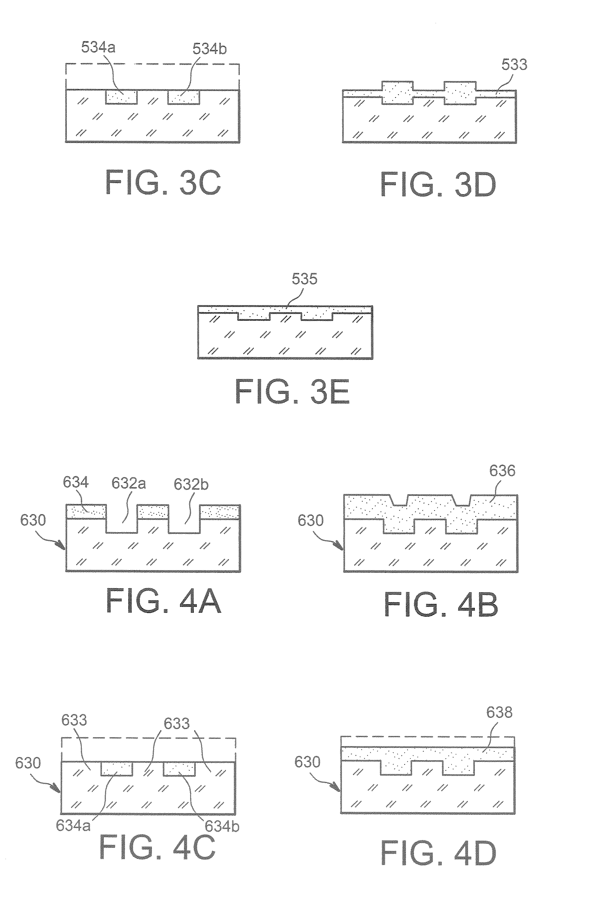
[0182]In this first example, the patterns are etched with a reactive ion etching (RIE) type method and have a depth of 50 nanometers in the silicon.

[0183]The SiO2 oxide is generated in these patterns and above the bridges by a heat treatment at 900° C. under a steam atmosphere. Its thickness is 120 nanometers (FIG. 6A).

[0184]A SiO2 film of 150 nm is deposited by PECVD at the surface of the thermal oxide film (FIG. 6B). The topology (surface relief) may be suppressed by CMP polishing. The surface is then smoothed and the deposited oxide film is polished up to the point where the thermal oxide emerges, the beginning of the so-called mixed oxide area (FIG. 6C).

[0185]Densification of the deposited oxide is performed at 900° C. under an oxygen atmosphere for 1 hr.

[0186]Complementary thinning is carried out for example by CMP or by HF etching (HF diluted to 10% or even 1%) or by reactive ionic etching, in a CHF3 plasma for example. The complementary thinning causes no or little > between ...

second example

[0190]In this second example, the patterns are etched with a reactive ion etching (RIE) type method and have a depth of 50 nanometers in the silicon. The oxide is generated in these patterns and above the bridges by heat treatment at 900° C. under a steam atmosphere. Its thickness is 120 nanometers (FIG. 6A).

[0191]A 150 nm SiO2 film is deposited by PECVD at the surface of the thermal oxide film. The topology (surface relief) may be suppressed by CMP polishing. The surface is smoothed and the deposited oxide film is polished up to the point where the thermal oxide emerges, the beginning of the so-called mixed oxide area (FIG. 6C).

[0192]Densification of the deposited oxide is performed at 900° C. under an oxygen atmosphere for 1 hr.

[0193]Complementary thinning is for example carried out by CMP or by HF etching (HF diluted to 10% or even 1%) or by reactive ionic etching, in a CHF3 plasma for example. The complementary thinning causes no or little dishing between the areas of different ...

third example

[0196]In this third example, the patterns are etched with a reactive ion etching (RIE) type method and have a depth of 50 nanometers in the silicon. The oxide is generated in these patterns and above the bridges by a heat treatment at 900° C. under a steam atmosphere. Its thickness is 120 nanometers (FIG. 6A).

[0197]A 150 nm SiO2 film is deposited by PECVD at the surface of the thermal oxide film. The topology (surface relief) may be suppressed by CMP polishing. The surface is smoothed and the deposited oxide film is polished up to the point where the thermal oxide emerges, the beginning of the so-called mixed oxide area (FIG. 6C).

[0198]Densification of the deposited oxide is performed at 900° C. under an oxygen atmosphere for 1 hr.

[0199]Complementary thinning is for example carried out by CMP or by HF etching (HF diluted to 10% or even 1%) or by reactive ionic etching, in a CHF3 plasma for example. The complementary thinning causes no or little dishing between the areas of different...


PUM

PropertyMeasurementUnit
depthaaaaaaaaaa
depthaaaaaaaaaa
widthaaaaaaaaaa

Abstract

The invention relates to a method for producing a semiconducting structure on a semiconducting substrate, one surface of which has a topology, this method including:a) a step for forming a first layer (24) in a first insulating material on said surface,b) a step for forming a second layer in a second insulating material (28), less dense than the first insulating material, with a thickness between 2.5 p and 3.5 p,c) a step for planarization of the assembly.

Description

TECHNICAL FIELD AND PRIOR ART[0001]The invention relates to the field of semiconductor-on-insulator type structures, such as for silicon-on-insulator also designated as SOI, structures.[0002]In these technologies, a substrate of material, generally a semiconducting material, supports a buried insulator film, for example in silicon dioxide, and a film of superficial semiconducting material.[0003]Producing such semiconductor-on-insulator structures is possible by means of several technologies, such as for example described in the book of Q. Y. Tong and U. Gösele, <<Semiconductor wafer bonding, Science and technology >>, Ed. The Electrochemical Society Series, 1999:[0004]by means of methods based on implanting oxygen in a semiconducting material and on heat treatment(s) at high temperatures (methods of the SIMOX type),[0005]by means of methods based or molecular bonding and with, for example, i.e.:[0006]mechanical and / or chemical thinning (methods of the BSOI type,[0007]mec...

Claims


Application Information

Patent Timeline
Patent Type & Authority Patents(United States)
IPC IPC(8): H01L21/30H01L21/46
CPCH01L21/7624H01L21/76251H01L21/76254H01L21/76259
Inventor MORICEAU, HUBERTMORALES, CHRISTOPHEZUSSY, MARCDECHAMP, JEROME
Owner COMMISSARIAT A LENERGIE ATOMIQUE ET AUX ENERGIES ALTERNATIVES
Why Eureka
Try Eureka