Chemical-enhanced package singulation process

a technology of chemical enhancement and package, applied in the direction of semiconductor devices, semiconductor/solid-state device details, electrical equipment, etc., can solve the problems of residual electrical charge, short-out or otherwise disrupting electrical connections, and low throughpu

Active Publication Date: 2009-06-30
GEM SERVICES
View PDF12 Cites 0 Cited by
  • Summary
  • Abstract
  • Description
  • Claims
  • Application Information

AI Technical Summary

Problems solved by technology

However, this conventional singulation process offers a number of potential disadvantages.
One such disadvantage is relatively low throughput.
In particular, rapid sawing of the metal can generate residual electrical charge that can short-out or otherwise disrupt the electrical connections carefully fabricated within the packages.

Method used


Image

  • Chemical-enhanced package singulation process
  • Chemical-enhanced package singulation process
  • Chemical-enhanced package singulation process

Examples


Embodiment Construction

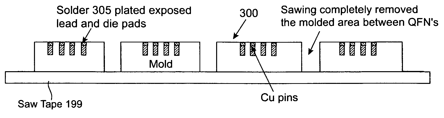
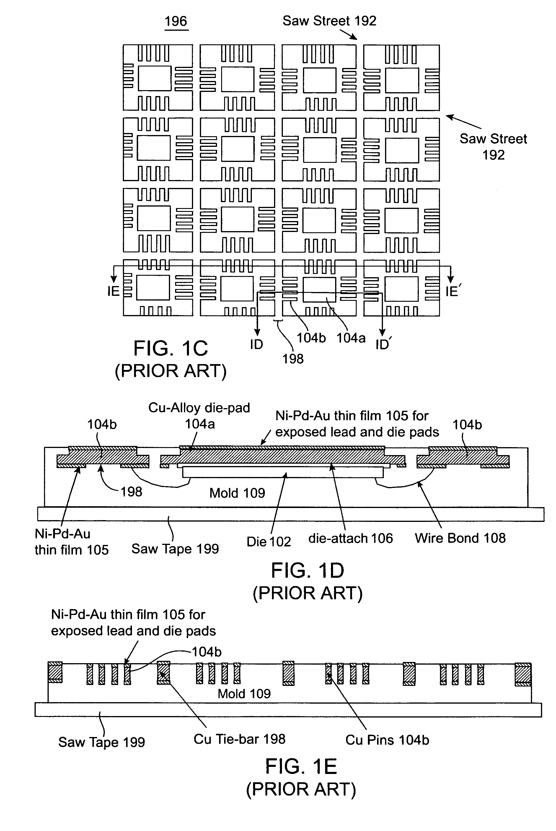
[0027]Physical singulation of individual electronic packages fabricated as part of a larger matrix, is accomplished by sawing in combination with chemical exposure and patterning of a mask. In one embodiment of a singulation process in accordance with the present invention, an initial, shallow saw cut into inter-package portions of the matrix exposes underlying metal to subsequent chemical etching steps. In an alternative embodiment of a singulation process in accordance with the present invention, a separate photoresist mask may be patterned over the matrix to selectively expose metal in inter-package regions to chemical etching.

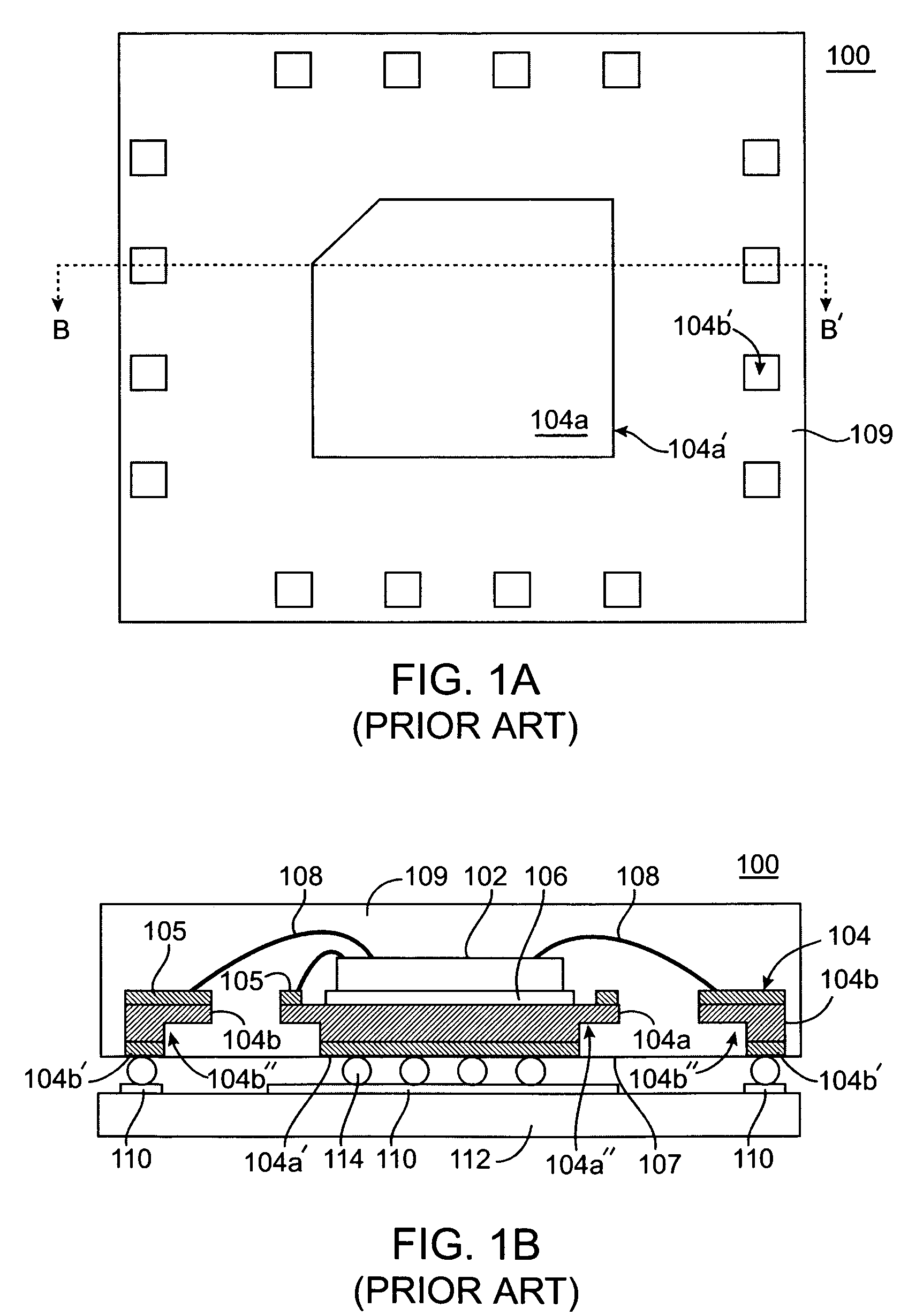
[0028]U.S. Nonprovisional patent application Ser. No. 10 / 751,265 is incorporated herein by reference for all purposes, describes the use of electroplating techniques to form package features. Embodiments of singulation processes in accordance with the present invention may be used to fabricate packages as described in that patent application.

[0029]A discuss...


PUM


Abstract

Singulation of individual electronic packages fabricated as part of a common matrix, is accomplished by mask patterning and chemical exposure in combination with physical sawing. In one embodiment of a singulation process in accordance with the present invention, an initial, shallow saw cut into inter-package regions of the matrix exposes underlying metal to subsequent chemical etching steps. In an alternative embodiment, a separate photoresist mask may be patterned over the matrix to selectively expose metal in inter-package regions to chemical etching.

Description

BACKGROUND OF THE INVENTION[0001]FIG. 1A shows an underside plan view of a conventional quad flat no-lead (QFN) package utilized to house a semiconductor device. FIG. 1B shows a cross-sectional view taken along line B-B′, of the conventional QFN package of FIG. 1A, positioned on a PC board.[0002]QFN package 100 comprises semiconductor die 102 having electrically active structures fabricated thereon. Die 102 is affixed to underlying diepad 104a portion of lead frame 104 by die attach adhesive 106. The relative thickness of the die and lead frame shown in FIG. 1B, and all other drawings of this patent application, is not to scale. Lead frame 104 also comprises non-integral pin portions 104b in electrical communication with die 102 through bond wires 108. Bond wires 108 also allow electrical communication between die 102 and diepad 104a. [0003]Plastic molding 109 encapsulates all but the exposed portions 104a′ and 104b′ of the lead frame portions 104a and 104b, respectively. For the pu...

Claims


Application Information

Patent Timeline
Patent Type & Authority Patents(United States)
IPC IPC(8): H01L21/44H01L21/68H01L23/31H01L23/495
CPCH01L21/6835H01L23/3107H01L23/49548H01L24/97H01L2221/68331H01L2224/48247H01L2224/48257H01L2224/73265H01L2224/97H01L2924/01011H01L2924/01015H01L2924/01029H01L2924/01033H01L2924/01046H01L2924/01047H01L2924/01075H01L2924/01078H01L2924/01079H01L2924/01082H01L2924/15311H01L24/48H01L2924/01005H01L2924/01006H01L2924/01019H01L2224/32245H01L2924/00H01L2924/181H01L2924/00014H01L2924/18301H01L2924/00012H01L2224/45099H01L2224/45015H01L2924/207
Inventor YILMAZ, HAMZACHIA, ANTHONYZENG, XIAOGUANGMING, WONG HIEWANG, LIMINGZHANG, YIJU
Owner GEM SERVICES
Why Eureka
Try Eureka