High speed analog envelope detector

an envelope detector, high-speed technology, applied in the direction of pulse manipulation, pulse technique, instruments, etc., can solve the problems of increasing the number of wires required and the weight and size of cables, affecting the power efficiency of the system, and increasing the amount of wires required

Active Publication Date: 2009-07-07
SAMSUNG ELECTRONICS CO LTD
View PDF19 Cites 35 Cited by
  • Summary
  • Abstract
  • Description
  • Claims
  • Application Information

AI Technical Summary

Benefits of technology

[0018]A high speed (HS) transmission envelope detector (e.g., for use in an analog front end of a USB2.0 transceiver) according to a preferred embodiment of the invention generates first through fourth level-shifted signals in response to differential input signals (e.g., that are received from an external device), the first through fourth level-shifted signals having voltage levels higher than the differential input signal. After comparing the first through fourth level-shifted signals with each other, the compared result is used in determining the validity of data transmitted in the differential input signals. The transmission envelope detector flexibly adapts to variations of the common mode voltage, and simplifies the circuit architecture, (e.g., because it does not need an additional reference voltage for determining the data validity).

Problems solved by technology

Parallel interfacing schemes offer sufficient bandwidth, but there is a disadvantage of too large a data width which increases the number of wires required and the weight and size of cables.
And, if the number of signal lines increases in small apparatuses such as mobile phones, electro-magnetic interference (EMI) increases as well as degradation of power efficiency.
And, the increased number of signal lines occupies more space for the signal lines, making it difficult to miniaturize the small apparatuses.
However, when using the external reference voltage, it is difficult to deal with common-mode (CM) voltage variation because the reference voltage level is independent and fixed.
And it is complicated to construct the circuit due to additional structures of a first differential amplifier to amplify a difference between a reference voltage and an input signal received from the D+ line, and a second differential amplifier to amplify a difference between the reference voltage and an input signal received from the D− line.
Thus, settling a CM voltage takes a long time, and constructing the circuit is complicated as well.

Method used


Image

  • High speed analog envelope detector
  • High speed analog envelope detector
  • High speed analog envelope detector

Examples


Embodiment Construction

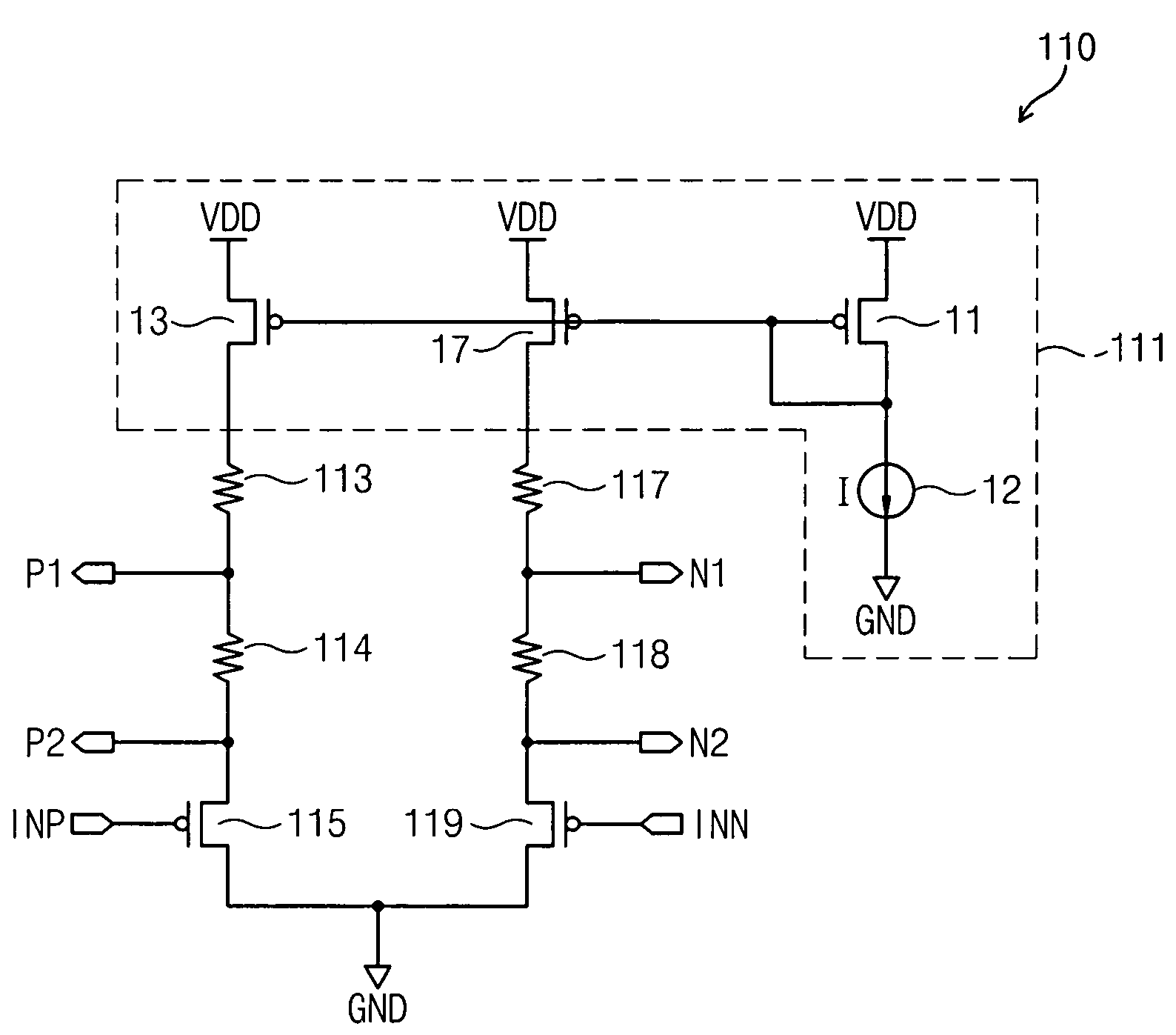
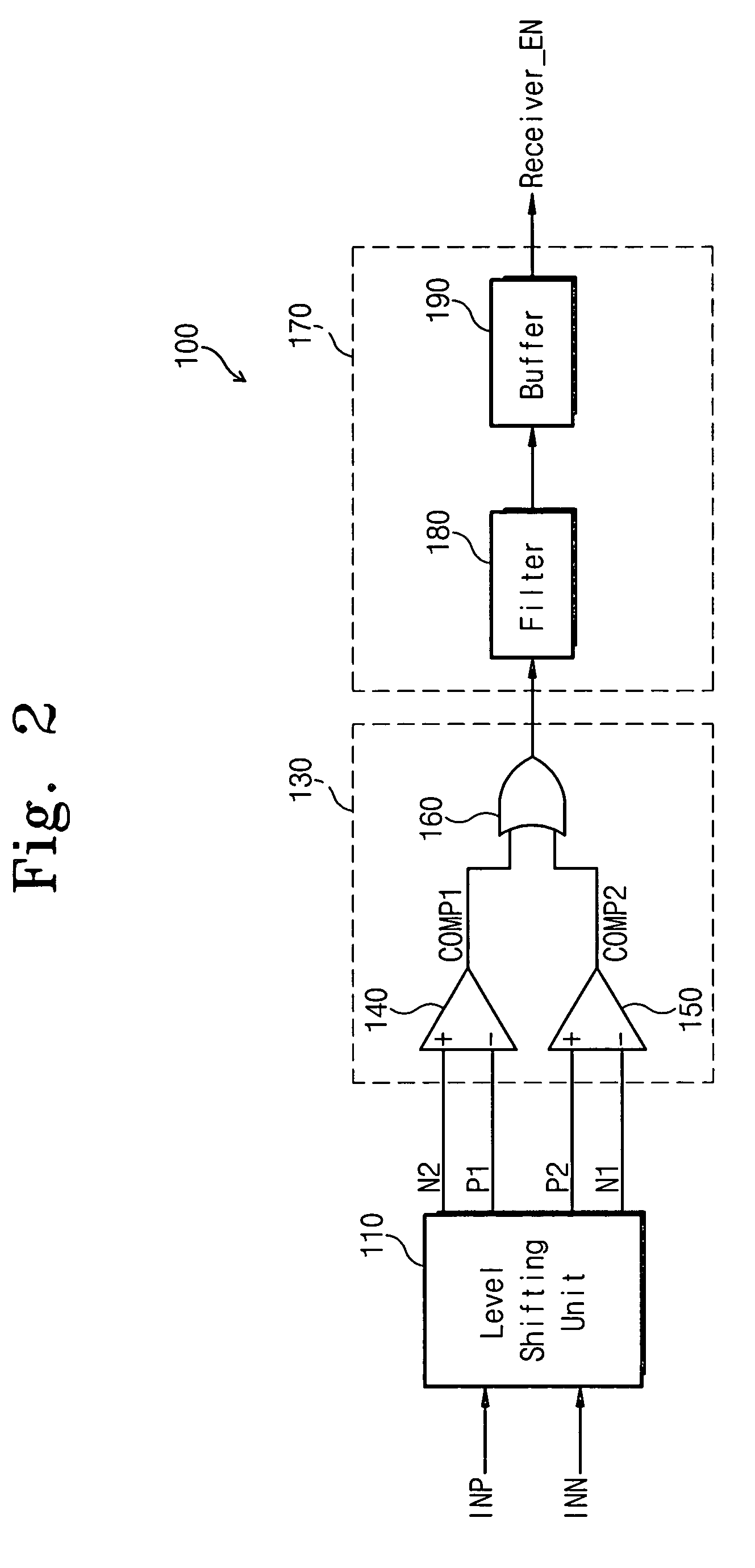
[0036]FIG. 2 is a block diagram of a transmission envelope detector 100 in accordance with a preferred embodiment of the invention.

[0037]Referring to FIG. 2, the envelope detector 100 is comprised of a level shifting unit 110, a comparing circuit 130, and an output signal conditioning circuit 170. The level shifting unit 110 generates first through fourth level-shifted signals P1, P2, N1, and N2 having voltage levels higher than differential input signals INP and INN, in responds to the differential input signals INP and INN that are received (e.g., from an external device via USB cables).

[0038]The first and second level-shifted signals P1 and P2 are generated in response to the differential input signal INP having a positive value. The third and fourth level-shifted signals, N1 and N2, are generated in response to the differential input signal INN having a negative value. The first level-shifted signal P1 has a voltage level higher than that of the second level-shifted signal P2. T...


PUM


Abstract

A high speed analog transmission envelope (data-validity) detector for detecting the validity or invalidity of received data by generating (and comparing) first through fourth level-shifted signals based on a pair of differential input signals that are externally applied (received). Each of the first through fourth level-shifted signals has voltage levels different from (e.g., higher than) the differential input signals. After comparing the first through fourth level-shifted signals with each other, the comparison results are used in determining the validity of the differential input signals (data). The analog transmission envelope (data) detector flexibly adapts to variations in common mode voltage, and simplifies the circuit architecture because it does not require an additional reference voltage for determining the validity of received data.

Description

CROSS-REFERENCE TO RELATED APPLICATIONS[0001]This U.S. non-provisional patent application claims priority under 35 U.S.C. § 119 of Korean Patent Application 2004-108790 filed on Dec. 20, 2004, the entire contents of which are hereby incorporated by reference.BACKGROUND OF THE INVENTION[0002]1. Field of the Invention[0003]The present invention relates to analog front ends for high speed serial communication and more particularly to analog transmission envelope detectors operable at the high frequencies of USB2.0.[0004]2. Description of the Related Art[0005]With increases in operating frequencies of central processing units (CPUs) of personal computers (PCs) on the order of several GHz, there have been proposed various high-frequency interfacing systems. For example, there are peripheral component interconnection (PCI) bus systems and IEEE 1284, as kinds of parallel interfacing schemes. Parallel interfacing schemes offer sufficient bandwidth, but there is a disadvantage of too large a...

Claims


Application Information

Patent Timeline
Patent Type & Authority Patents(United States)
IPC IPC(8): H03L5/00
CPCH03K5/2481H04L12/02
Inventor YU, JAE-SUK
Owner SAMSUNG ELECTRONICS CO LTD
Why Eureka
Try Eureka