
Scintillator material and radiation detectors containing same

a radiation detector and material technology, applied in the field of scintillator materials, can solve the problems of reducing image resolution, difficult to predict the change of any individual scintillator, and difficult to implement quantitative correction measures

Inactive Publication Date: 2009-07-14
GENERAL ELECTRIC CO
View PDF14 Cites 11 Cited by
  • Summary
  • Abstract
  • Description
  • Claims
  • Application Information

AI Technical Summary

Benefits of technology

[0016]Various configurations of the present invention provide short decay times and have reduced damage upon exposure to high-energy radiation relative to known scintillator compositions. Additionally, configurations of scintillator compositions of the present invention have higher densities than known scintillator compositions, thus providing a higher radiation stopping power to prevent damage to semiconductor detector arrays on which the scintillator compositions are deposited.

Problems solved by technology

Radiation damage can lead to “ghost images” from prior scans which thereby reduce image resolution.
The change in light output that occurs upon radiation damage is often found to be variable in magnitude from batch-to-batch of the same scintillator, making it difficult to predict how any individual scintillator will change over time and thus, making it difficult to implement quantitative correction measures.
This amount of variation in light output which can occur as a result of x ray damage is undesirable in a quantitative x ray detector.
Moreover current non-water soluble scintillator materials are difficult to manufacture, owing to their high melting points and the thickness of the scintillator coating that has to be applied to stop X-rays from reaching and damaging the detector.
The thick coatings also result in inefficient optical transmission.

Method used


Image

  • Scintillator material and radiation detectors containing same
  • Scintillator material and radiation detectors containing same

Examples


Embodiment Construction

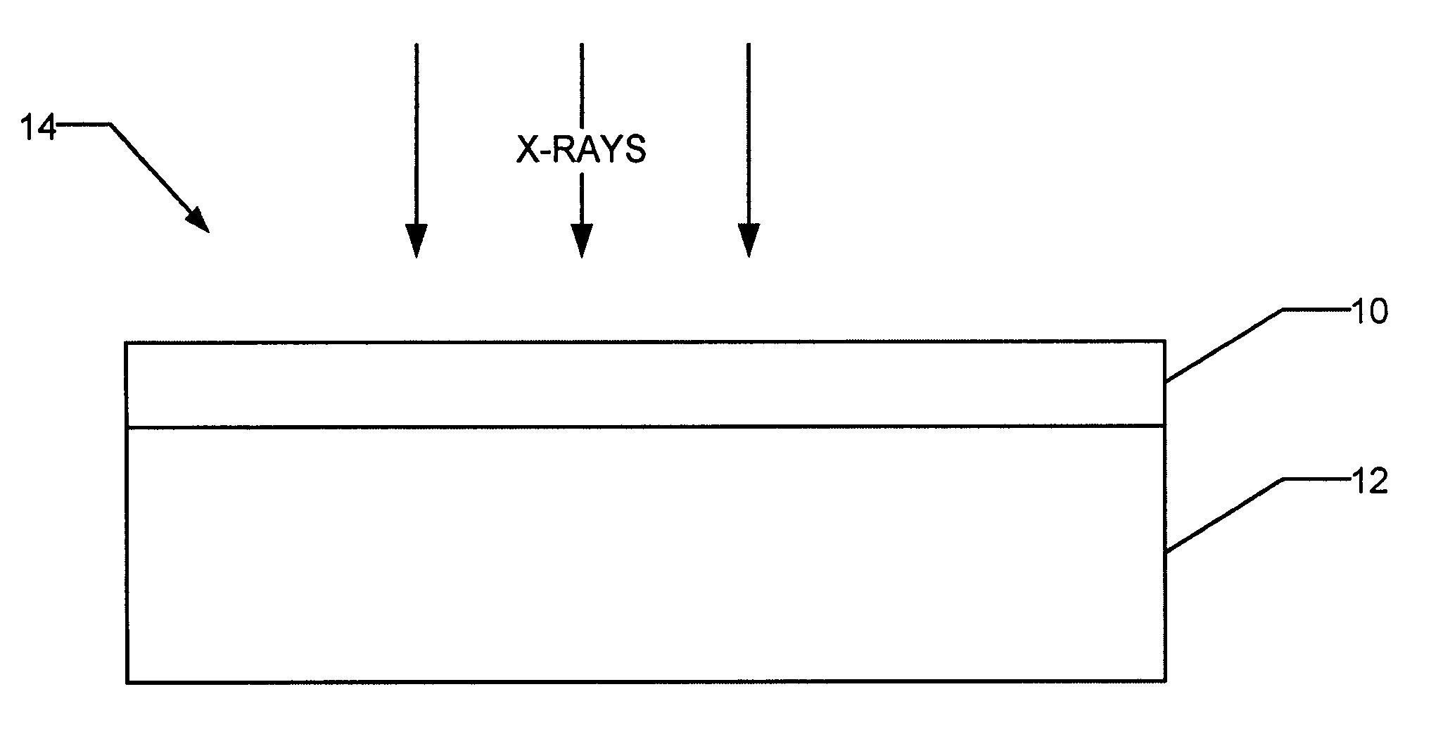
[0018]The terms “phosphor” and “scintillator” are used in an interchangeable way to mean a solid-state luminescent material that emits visible light in response to stimulation by high-energy radiation such as X, β, or γ radiation.

[0019]The term “high-energy radiation” means electromagnetic radiation having energy higher than that of ultraviolet radiation, including but not limited to, X radiation (also referred to as x ray radiation herein), gamma (γ) radiation, and beta (β) radiation. Solid-state scintillator materials are in common use as components of radiation detectors in apparatuses such as counters, image intensifiers, and computed tomography (“CT”) scanners.

[0020]The term “radiation damage” refers to the characteristic of a luminescent material in which the quantity of light emitted by the luminescent material in response to a given intensity of stimulating radiation changes after the material has been exposed to a high-energy radiation dose. The term “radiation damage” may ...


PUM

PropertyMeasurementUnit
timeaaaaaaaaaa
temperatureaaaaaaaaaa
timeaaaaaaaaaa

Abstract

A sintered, annealed scintillator composition, which, prior to annealing, has a formula of A3B2C3O12, where A is at least one member of the group consisting of Tb, Ce, and Lu, or combinations thereof, B is an octahedral site (Al), and C is a tetrahedral site (also Al). One or more substitutions are included. The substitutions may may be partial or, in some cases, complete, and can include Al with Sc at B, up to two atoms of oxygen with fluorine and the same number of Ca atoms at A, replacement at B with Mg and the same number of atoms of oxygen with fluorine, replacement at B with a combination of Mg / Si Mg / Zr, Mg / Ti, and / or Mg / Hf, replacement at B with a combination of Li / Nb and / or Li / Ta, and at A with Ca and replacement of an equal number of B or C with silicon.

Description

BACKGROUND OF THE INVENTION[0001]This invention relates generally to scintillator materials useful for radiation detectors and for radiation detectors made therewith, and more particularly to scintillator materials that can be used in thin slices and / or processed at a relatively low temperature, and radiation detectors made therewith.[0002]Solid state scintillator materials have long been used as radiation detectors to detect penetrating radiation in such applications as x ray counters and image intensifiers. The scintillator materials emit visible or near visible radiation when stimulated by x rays or other high energy electromagnetic photons. In typical medical or industrial applications, the optical output from the scintillator is directed to a photoelectrically responsive device to produce electrical output signals, where the amplitude of the signals is proportional to the deposited energy. The electrical signals can than be digitized by a computer for display on a screen or oth...

Claims


Application Information

Patent Timeline
Patent Type & Authority Patents(United States)
IPC IPC(8): C09K11/06C09K11/02C09K11/61C09K11/77
CPCC09K11/7774C04B35/44C04B2235/80C04B2235/3203C04B2235/3206C04B2235/3208C04B2235/3222C04B2235/3225C04B2235/3229C04B2235/3232C04B2235/3244C04B2235/3251C04B2235/3418C04B2235/445C04B2235/6565C04B2235/6567C04B2235/6584C04B2235/663C04B2235/764
Inventor LYONS, ROBERT JOSEPHVENKATARAMANI, VENKAT SUBRAMANIAMSETLUR, ANANT ACHYUT
Owner GENERAL ELECTRIC CO
Learn More