Package optical chip with conductive pillars

a technology of optical chips and conductive pillars, which is applied in the direction of electrical apparatus, semiconductor devices, semiconductor/solid-state device details, etc., can solve the problems of frame 150/b>, increase not only the but also the material cost, so as to reduce the cost and volume of the package structure

Active Publication Date: 2009-07-14
ADVANCED SEMICON ENG INC
View PDF9 Cites 26 Cited by
  • Summary
  • Abstract
  • Description
  • Claims
  • Application Information

AI Technical Summary

Benefits of technology

[0008]It is therefore an object of the invention to provide a package structure and a fabricating method thereof. An optical chip with a conductive pillar is used in the package structure of the invention, so that the optical chip is electrically connected to a board directly through the conductive pillar instead of wire bonding. Furthermore, a soft board is used in the package structure, and a transparent protection sheet is attached to the optical chip. Therefore, there is no need to use a frame. The cost and the volume of the package structure are both reduced. Moreover, the package structure can be bent to fit smaller space.

Problems solved by technology

As a result, the frame 150 increases not only the material cost but also the volume of the package structure 100.

Method used


Image

  • Package optical chip with conductive pillars
  • Package optical chip with conductive pillars
  • Package optical chip with conductive pillars

Examples


Embodiment Construction

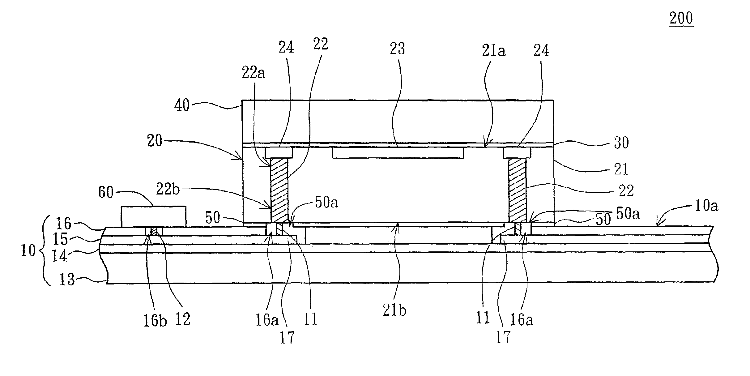
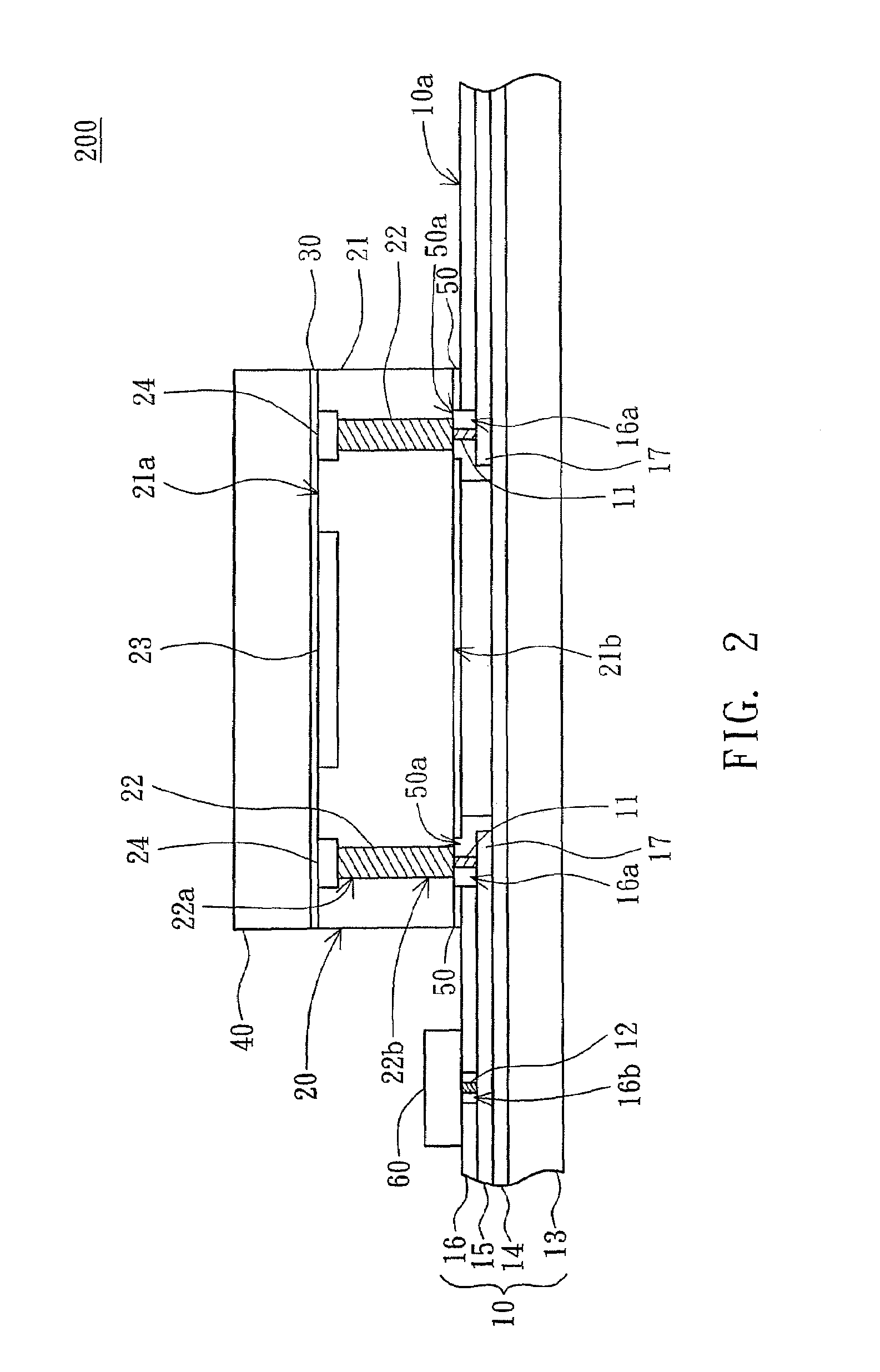
[0019]Please referring to FIG. 2, a package structure according to a preferred embodiment of the present invention is illustrated. A package structure 200 includes a soft board 10 and an optical chip 20. The optical chip 20 can be any kind of chip. For example, the optical chip 20 is a CMOS image sensor (CIS) in the present embodiment. The optical chip 20 is directly disposed on and electrically connected to the soft board 10.

[0020]The soft board 10 having a surface 10a includes a pad 17. At least a first bump 11 is disposed on the pad 17. In the present embodiment, two first bumps 11 are illustrated as an example. The optical chip 20 includes a main body 21 and at least a conductive pillar 22. The main body 21 has an active surface 21a and a non-active surface 21b opposite to the active surface 21a. The active surface 21a has a sensing area 23 and at least a contact pad 24 electrically connected the sensing area 23. In the present embodiment, two conductive pillars 22 and two conta...


PUM


Abstract

A package structure and a fabricating method thereof are provided. The package structure includes a soft board and an optical chip. The soft board has a surface with a bump disposed thereon. The optical chip includes a main body and a conductive pillar. The main body has an active surface and a non-active surface opposite to the active surface. The active surface has a sensing area and a contact pad electrically connected with each other. The non-active surface is attached to the surface. The conductive pillar is disposed inside the main body, and penetrates the active surface and the non-active surface. The conductive pillar has a first end electrically connected to the contact pad and a second end electrically connected to the bump.

Description

[0001]This application claims the benefit of Taiwan application Serial No. 095100112, filed Jan. 2, 2006, the subject matter of which is incorporated herein by reference.BACKGROUND OF THE INVENTION[0002]1. Field of the Invention[0003]The invention relates in general to a package structure and a fabricating method thereof, and more particularly to a package structure including an optical chip with a conductive pillar and a fabricating method thereof.[0004]2. Description of the Related Art[0005]With the rapid development of semiconductor packaging technology, all kinds of chips are packaged in order to protect the chips, prevent the chips from moisture and electrically connect inner wires of the chips and wires of printed circuit boards. Among all kinds of chips, the optical chip especially needs well protection to prevent its sensing area from particle pollution. A conventional package structure with an optical chip is illustrated as follow.[0006]FIG. 1 shows a conventional package s...

Claims


Application Information

Patent Timeline
Patent Type & Authority Patents(United States)
IPC IPC(8): H01L31/12
CPCH01L23/481H01L27/14618H01L24/90H01L2224/48091H01L24/48H01L2224/90H01L2224/48227H01L2924/00014H01L2224/45099H01L2224/45015H01L2924/207
Inventor HSIAO, WEI-MINYANG, KUO-PIN
Owner ADVANCED SEMICON ENG INC
Why Eureka
Try Eureka