
Image inspection device and image inspection method using the image inspection device

a technology of image inspection and inspection method, which is applied in the direction of measurement device, optical radiation measurement, instruments, etc., can solve the problems of not being able to pass through the shielded portion and inspection cannot be conducted in this portion, so as to prevent light from halving more readily

Inactive Publication Date: 2009-08-04
MITSUBISHI ELECTRIC CORP
View PDF4 Cites 1 Cited by
  • Summary
  • Abstract
  • Description
  • Claims
  • Application Information

AI Technical Summary

Benefits of technology

This approach enables stable and comprehensive inspection of semiconductor wafers across their entire surface, including the peripheral regions, by preventing halation and ensuring accurate detection of defects without interrupting the inspection process.

Problems solved by technology

However, because light is blocked by the fine adjustment stand 2 at the peripheral portion of the cell, light is not allowed to pass through this portion, which poses a problem that an inspection cannot be conducted in this portion.
Hence, when configured to conduct an inspection using transmitted light, light is not allowed to pass through the shielded portion.
This raises a problem that there is a portion where an inspection cannot be conducted.

Method used


Image

  • Image inspection device and image inspection method using the image inspection device
  • Image inspection device and image inspection method using the image inspection device
  • Image inspection device and image inspection method using the image inspection device

Examples


first embodiment

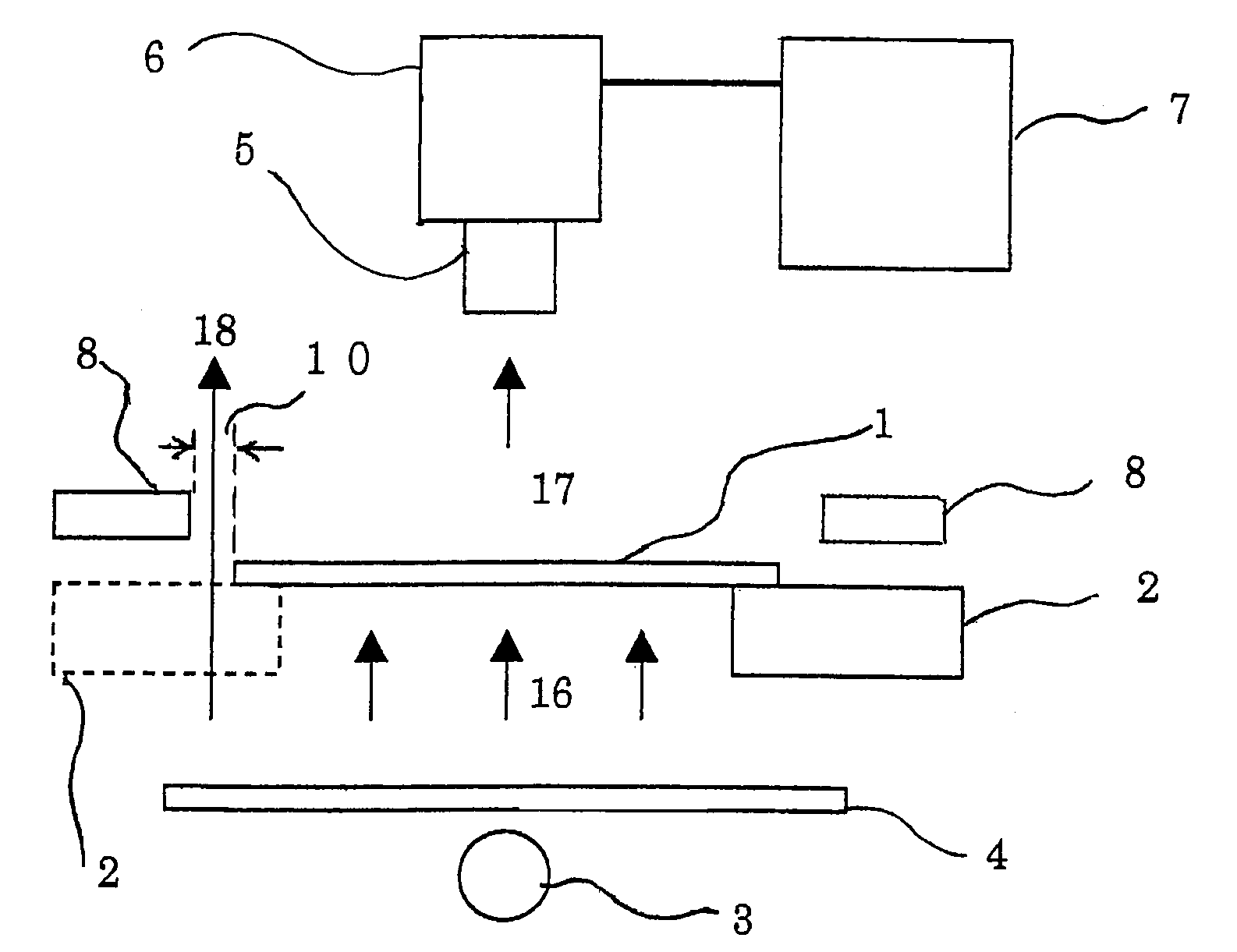
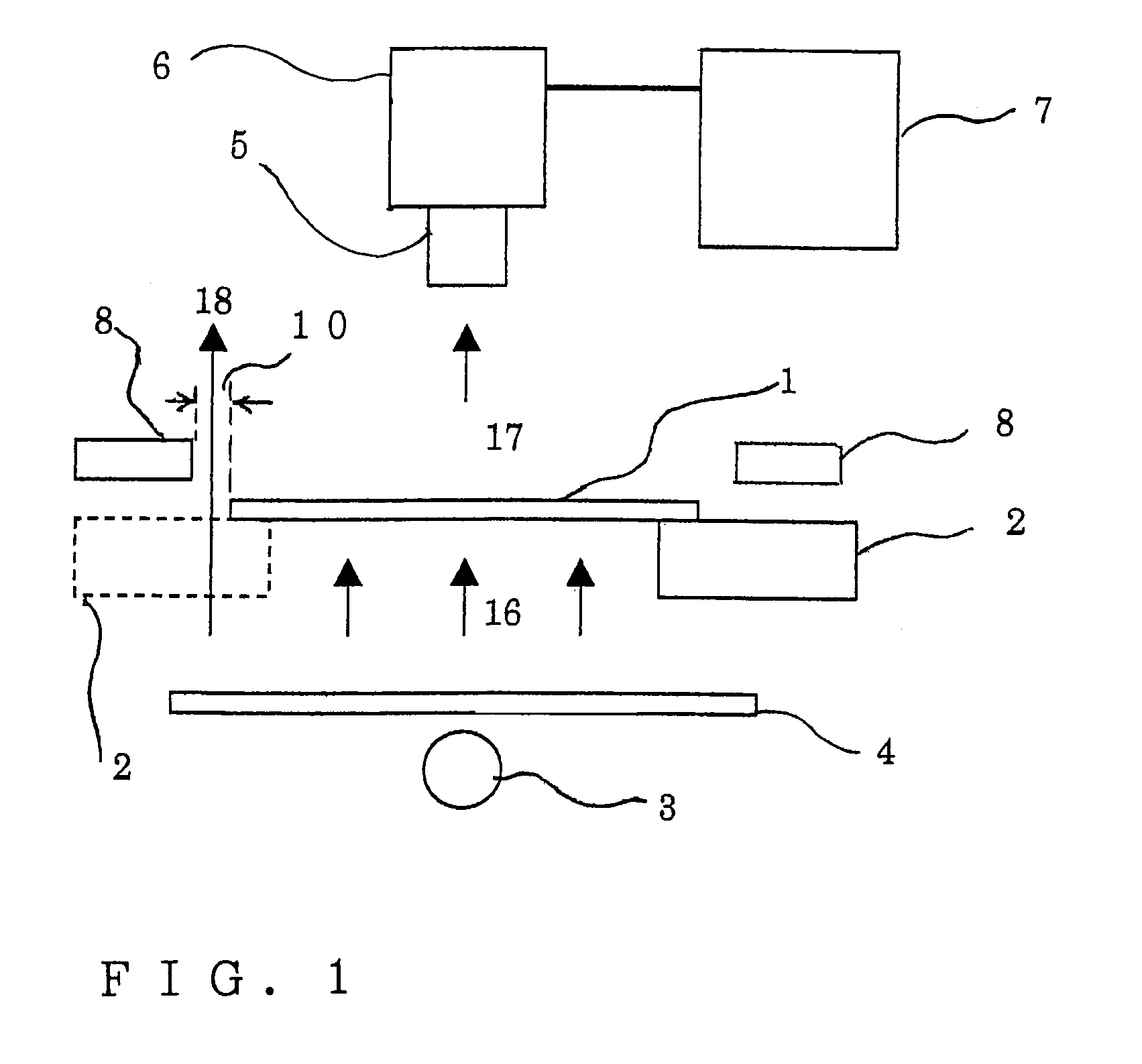
[0024]FIG. 1 is a view of the side surface showing the configuration of an image inspection device according to a first embodiment of the invention. Referring to the drawing, a holder stand 2 (referred to as the inspection object hold means) to hold a semiconductor wafer 1 (inspection object) that transmits infrared rays is provided on the lower side of the semiconductor wafer 1 so as to hold the semiconductor wafer 1 horizontally. Herein, descriptions will be given in a case where the outer shape of the semiconductor wafer 1 is a rectangle by way of example. An infrared light source 3 that irradiates infrared rays to an upper side is disposed below the semiconductor wafer 1, and a plate of an infrared diffusing medium 4 that diffuses infrared rays is provided above the infrared light source 3. The infrared diffusing medium 4 is furnished with a function of diffusing infrared rays homogeneously, and it is, for example, a translucent or frosted glass plate. Infrared rays after coming...

second embodiment

[0037]In FIG. 1 of the first embodiment, the mask 8 is illustrated as a thick plate-shaped member. However, as is shown in FIG. 6, because the end faces of the plate of the mask 8 are present at the position that can be viewed from the camera 6, light coming out from a translucent object 4 may possibly be reflected on the end faces (reflected light is denoted by 98 in the drawing) to come into the camera. In order to solve this problem, as is shown in FIG. 7, a non-reflecting mask 80 is used herein, which is structured to have sharp edges 80a formed in a thin and sharply pointed shape as the end faces and inclined portions 80b, so that extra light will not be reflected in a direction toward the semiconductor wafer 1 and the infrared camera 6. Because the sharp edges 80a are too thin for light to be reflected, no reflected light goes into the camera. In addition, the inclined portions 80b prevent extra reflected light from reaching the camera. It is thus possible to obtain a more sat...

third embodiment

[0038]The first embodiment and the second embodiment have described a case where the infrared diffusing medium 4 is provided horizontally. However, as is shown in FIG. 8, the infrared diffusing medium 4 may be provided at a specific angle, for example, an angle of 5° to 60° with respect to the horizontal level. By providing the infrared diffusing medium 4 at a specific angle, it is possible to prevent dirt, pieces of the semiconductor wafer, or the like from deposing on the infrared diffusing medium 4. This prevents dirt, pieces or the like accumulating on the top surface of the translucent object 4 from showing up in an image taken by the infrared camera 6. Hence, by eliminating a false recognition of a crack, it is possible to conduct an inspection for a crack in a more stable manner.


PUM


Abstract

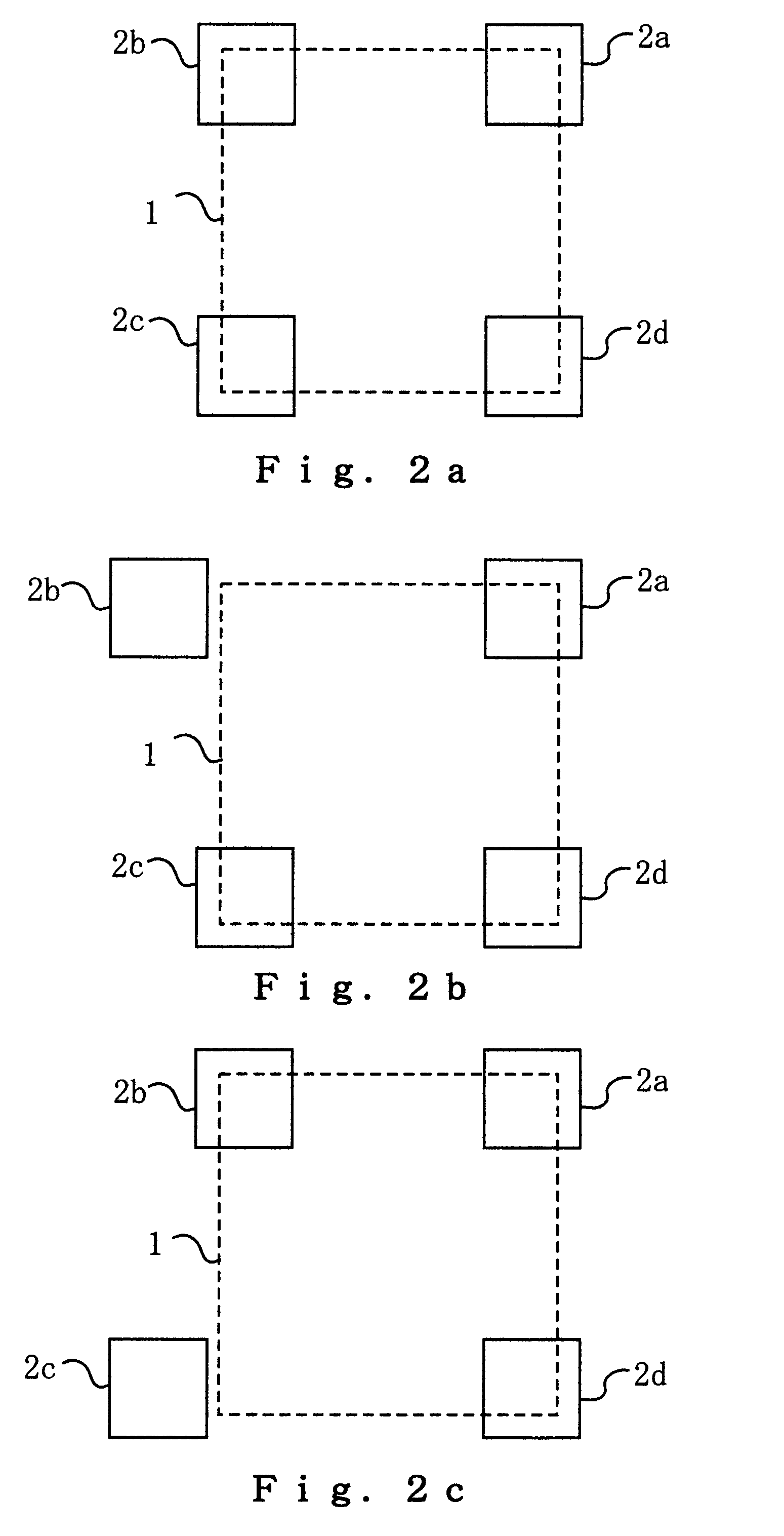
In an inspection of a semiconductor wafer for a defect, when infrared light passing through a semiconductor wafer is imaged by a camera and an inspection is conducted using the image, a problem that halation occurs in the camera due to light leaking from the side of the inspection object, which makes it impossible to conduct an inspection at the periphery portion occurs. An inspection object is irradiated by an infrared light source, and transmitted light is imaged by an infrared camera to be conducted. With the use of mask means that secures a clearance from the end portion on the outer side, it is possible to inspect on the peripheral portion. Also, as means for supporting the object, plural sets of those configured to be capable of evacuating are used, and by allowing the plural sets to evacuate alternately, it is possible to inspect across the entire surface.

Description

BACKGROUND OF THE INVENTION[0001]1. Field of the Invention[0002]The present invention relates to improvements of an image inspection method and an image inspection device for inspecting an inspection object for a defect from an image by taking an image of a plate-shaped inspection object having a property of transmitting infrared rays, for example, like a semiconductor wafer, using infrared rays.[0003]2. Description of the Related Art[0004]There is a device that inspects a plate-shaped transparent or translucent inspection object, such as a semiconductor wafer and a liquid crystal panel, for a defect (crack or adhesion of foreign matter) using light. Herein, for ease of description, a case where the inspection object is a semiconductor wafer will be described. It should be appreciated, however, that application of the invention is not limited to a semiconductor wafer (occasionally, referred to also as a cell). For example, JP-A-8-220008 discloses an inspection device that detects a ...

Claims


Application Information

Patent Timeline
Patent Type & Authority Patents(United States)
IPC IPC(8): G01J5/02
CPCG01N21/9505G01N21/9503
Inventor NISHINO, HIROHISAOHARA, TAKAOUNO, MASAHIKO
Owner MITSUBISHI ELECTRIC CORP
Learn More