Method for correcting eclipse or darkle

a technology of eclipse or darkle and image sensor, which is applied in the field of cmos image sensor, can solve the problems of difficult sensitivity to strong light when it shines onto the pixel array, and the inability to fit a single column circuit in the width of a single pixel, so as to prevent structure noise and preserve the simplicity and balance of the layout of the column circui

Active Publication Date: 2009-08-11
OMNIVISION TECH INC
View PDF12 Cites 28 Cited by
  • Summary
  • Abstract
  • Description
  • Claims
  • Application Information

AI Technical Summary

Benefits of technology

[0006]An advantage of this invention is the preservation of the simplicity and the balance of the layout of the column circuit. This will prevent structure noise from occurring in the image while successfully addressing the eclipse or darkle issue.

Problems solved by technology

A disadvantage of CMOS image sensors is its sensitivity to strong light when it shines onto the pixel array.
A typical example of this problem is when the camera is pointed directly to the sun; the sensor will output a “black” sun instead of a bright one in the image.
As the pixel pitch gets smaller, it may not be feasible to fit a single column circuit in the width of a single pixel.
In this case, including the correction feature will make the layout of the column circuit extremely challenging.
The imbalance created by including this feature will worsen the mismatch between the columns.

Method used


Image

  • Method for correcting eclipse or darkle
  • Method for correcting eclipse or darkle
  • Method for correcting eclipse or darkle

Examples


Embodiment Construction

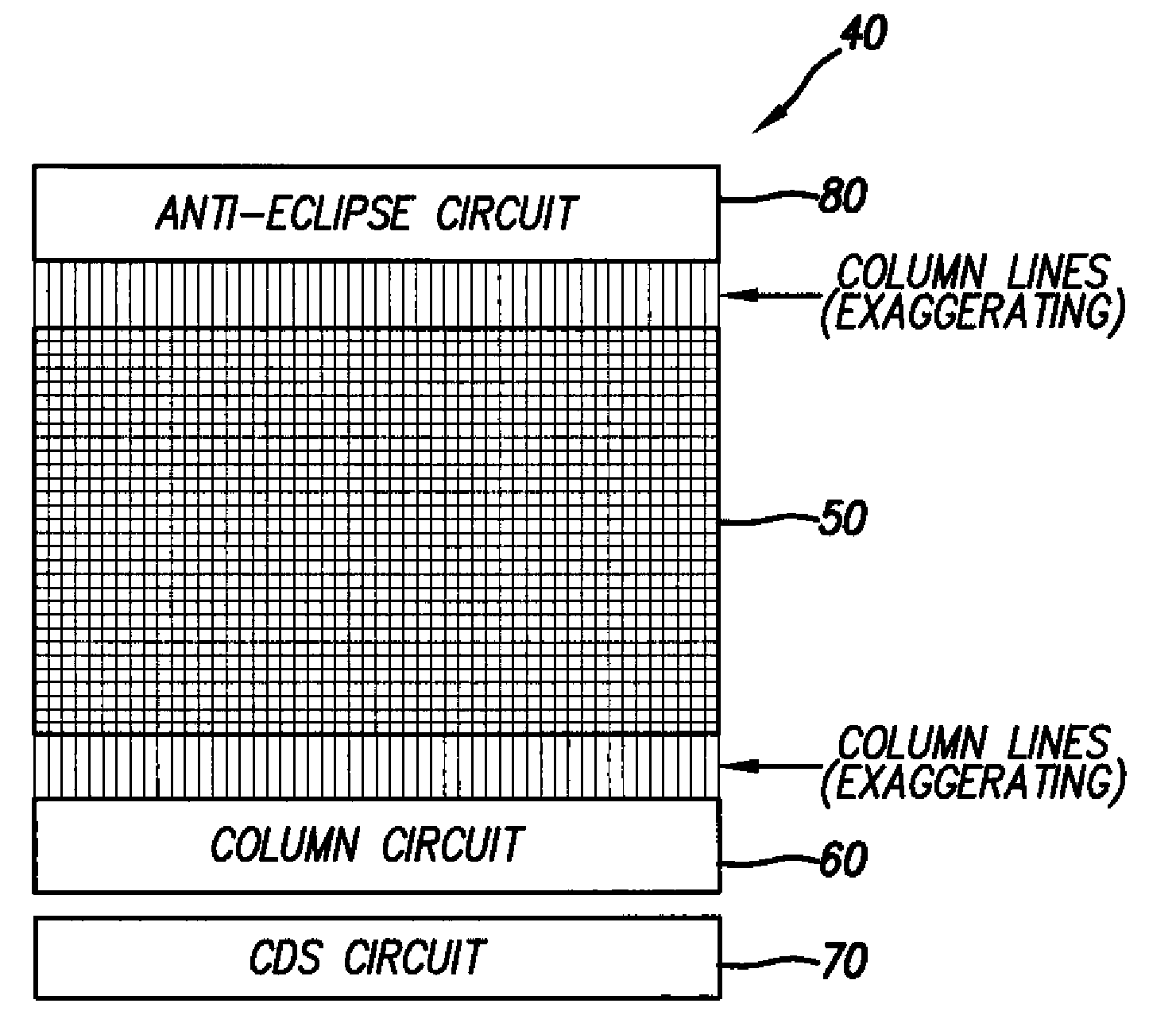
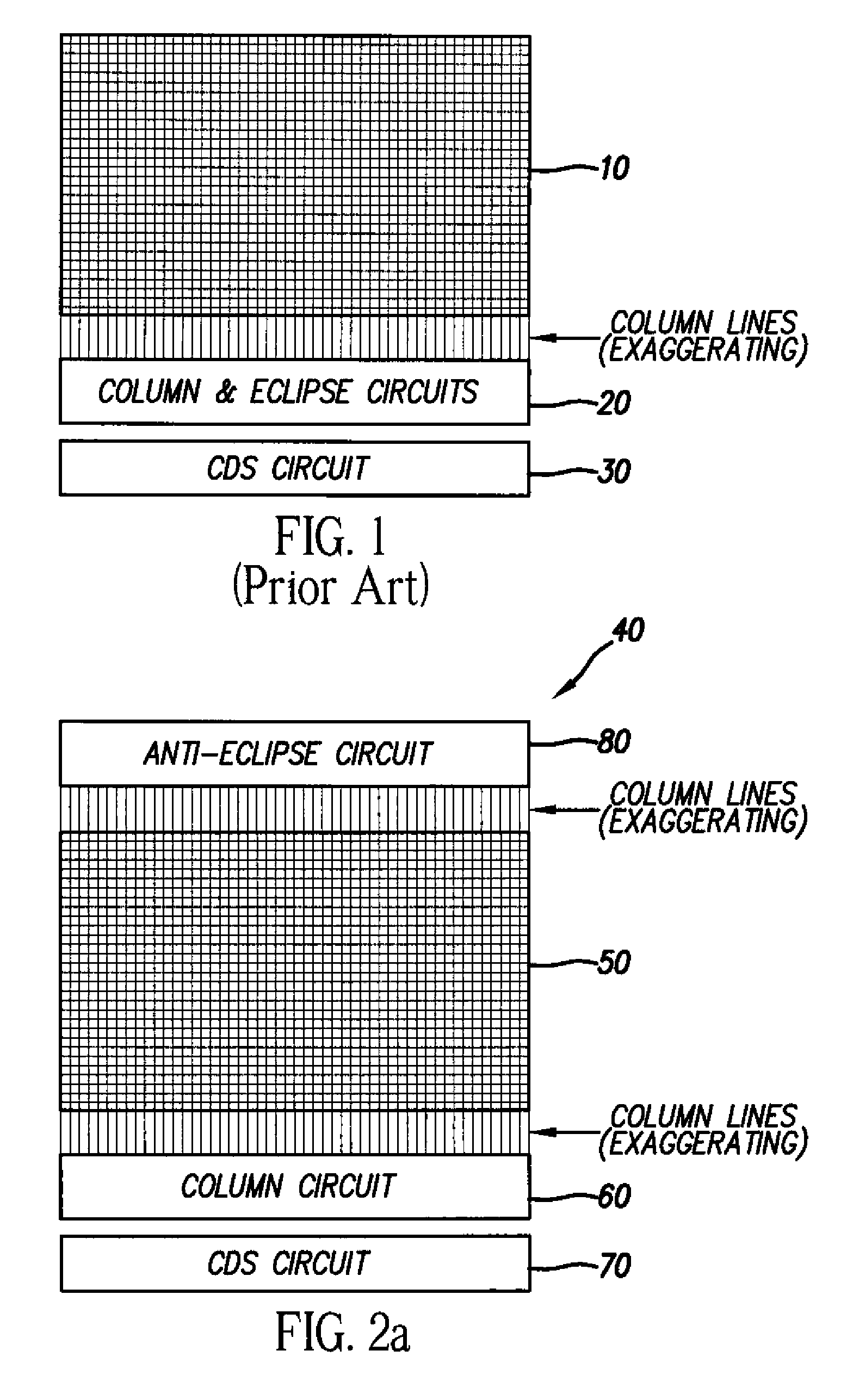
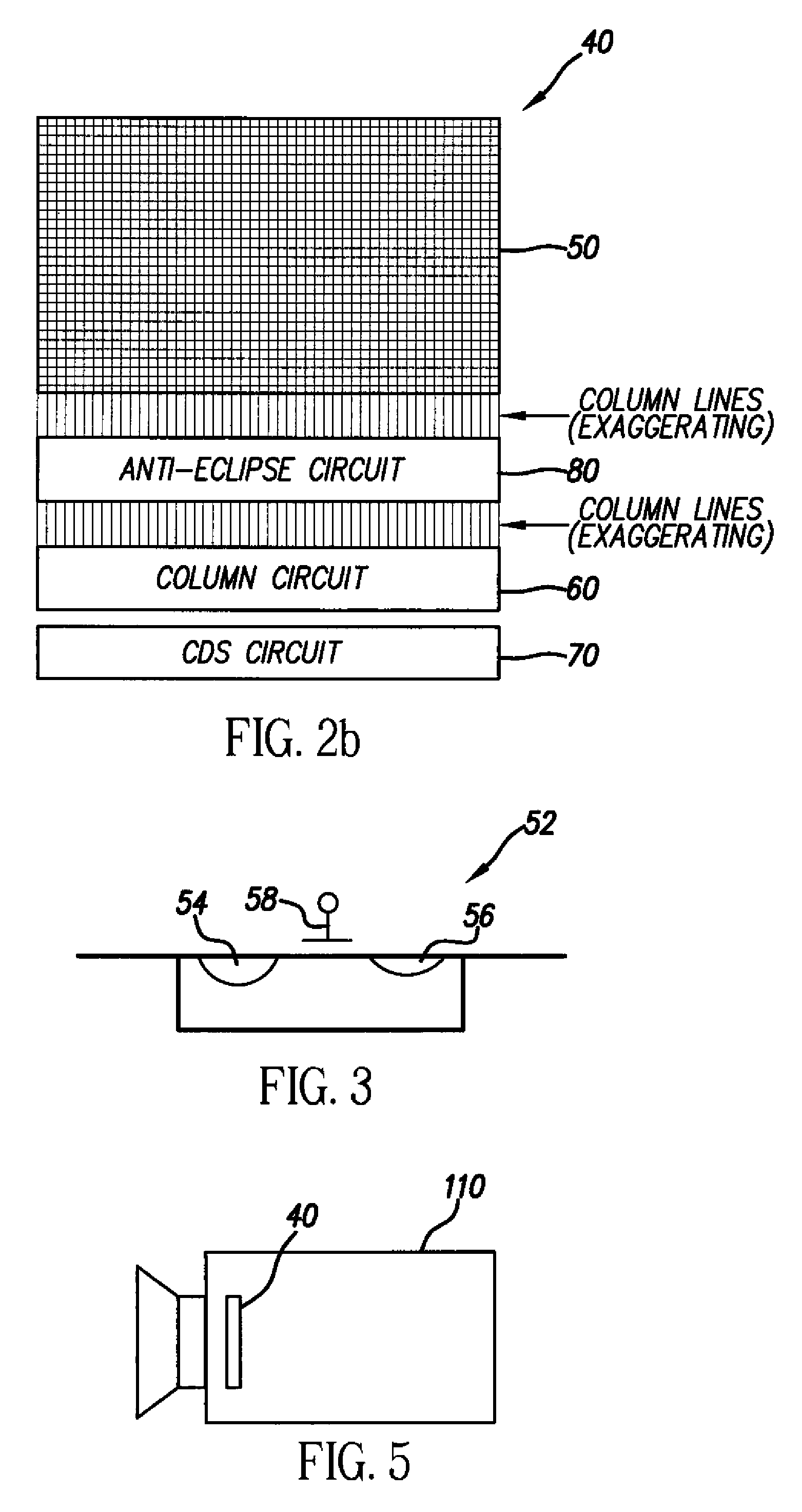
[0013]Referring to FIG. 2a, there is shown the image sensor 40 of the present invention that includes a plurality of pixels arranged in a two-dimensional array 50. Referring briefly to FIG. 3, each pixel 52 includes preferably either a pinned photodiode or a photodiode (sensing region 54) that is exposed to incident light for a desired period of time, referred to as integration, which causes charge to be collected within the sensing region 54. The pixel 52 also includes charge-to-voltage conversion circuitry 56 that receives the charge from the sensing region through a transfer gate 58 and converts the charge to a voltage, which will be referenced herein as the sample image signal.

[0014]Referring back to FIG. 2a, the operation of the image sensor includes two basic operations, reset and the above-mentioned integration. During the reset phase, the photodiode is set to a known reference voltage, often referred to as a reset level. Depending on the light intensity, this reset level is ...


PUM


Abstract

A CMOS image sensor includes a plurality of pixels arranged column and rows in an array; a column circuit for storing reset values and a value after integration; a correlated double sampler which derives an image signal from the reset and the value after integration; and an anti-eclipse circuit physically separately from the column circuit and electrically connected to one or shared between multiple columns of pixels for restoring corrupted column voltage on a column of pixels.

Description

FIELD OF THE INVENTION[0001]The present invention relates generally to the field of CMOS image sensors, and more particularly, to such image sensors having an anti-eclipse circuit for addressing reset problems. The anti-eclipse circuit is physically separated from a column circuit for preventing undesirable noise in captured images.BACKGROUND OF THE INVENTION[0002]A disadvantage of CMOS image sensors is its sensitivity to strong light when it shines onto the pixel array. A typical example of this problem is when the camera is pointed directly to the sun; the sensor will output a “black” sun instead of a bright one in the image. This phenomenon is referred to as eclipse or darkle. U.S. Ser. No. 10 / 607,943, filed Jun. 27, 2003, entitled “CMOS Image Sensor Oversaturation Protection Circuit,” by Christina Phan et al., addresses this problem. Referring to FIG. 1, there is shown a pixel array 10, column and eclipse circuit 20, and a correlated double sampler circuit 30. This prior art tec...

Claims


Application Information

Patent Timeline
Patent Type & Authority Patents(United States)
IPC IPC(8): H04N5/335H01L27/00H04N5/217H04N9/64H04N5/359H04N5/374H04N5/378
CPCH04N5/3598H04N25/627H04N25/60H04N25/75
Inventor PHAN, CHRISTINACAZZANIGA, MARCO
Owner OMNIVISION TECH INC
Why Eureka
Try Eureka