

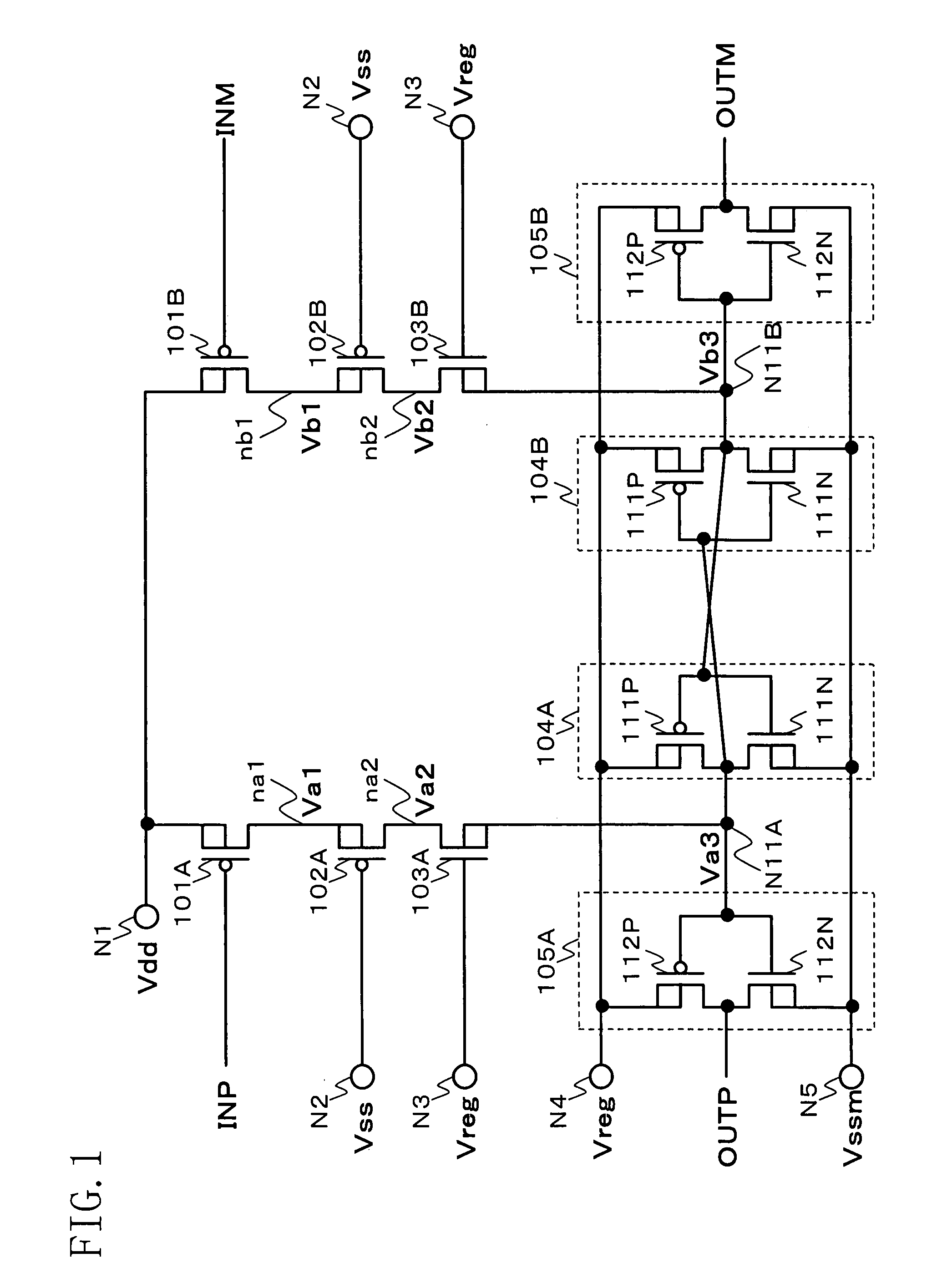
Level shifter
a level shifter and level shifter technology, applied in logic circuits, pulse automatic control, pulse technique, etc., can solve the problems of high breakdown voltage of the resistor, increase in cost or circuit area, increase in voltage variation rate at the output node, and reduce the source-drain voltage. , the effect of increasing the voltage variation ra
- Summary
- Abstract
- Description
- Claims
- Application Information
AI Technical Summary
Benefits of technology
Problems solved by technology
Method used
Image

Examples
first embodiment
Variation of First Embodiment
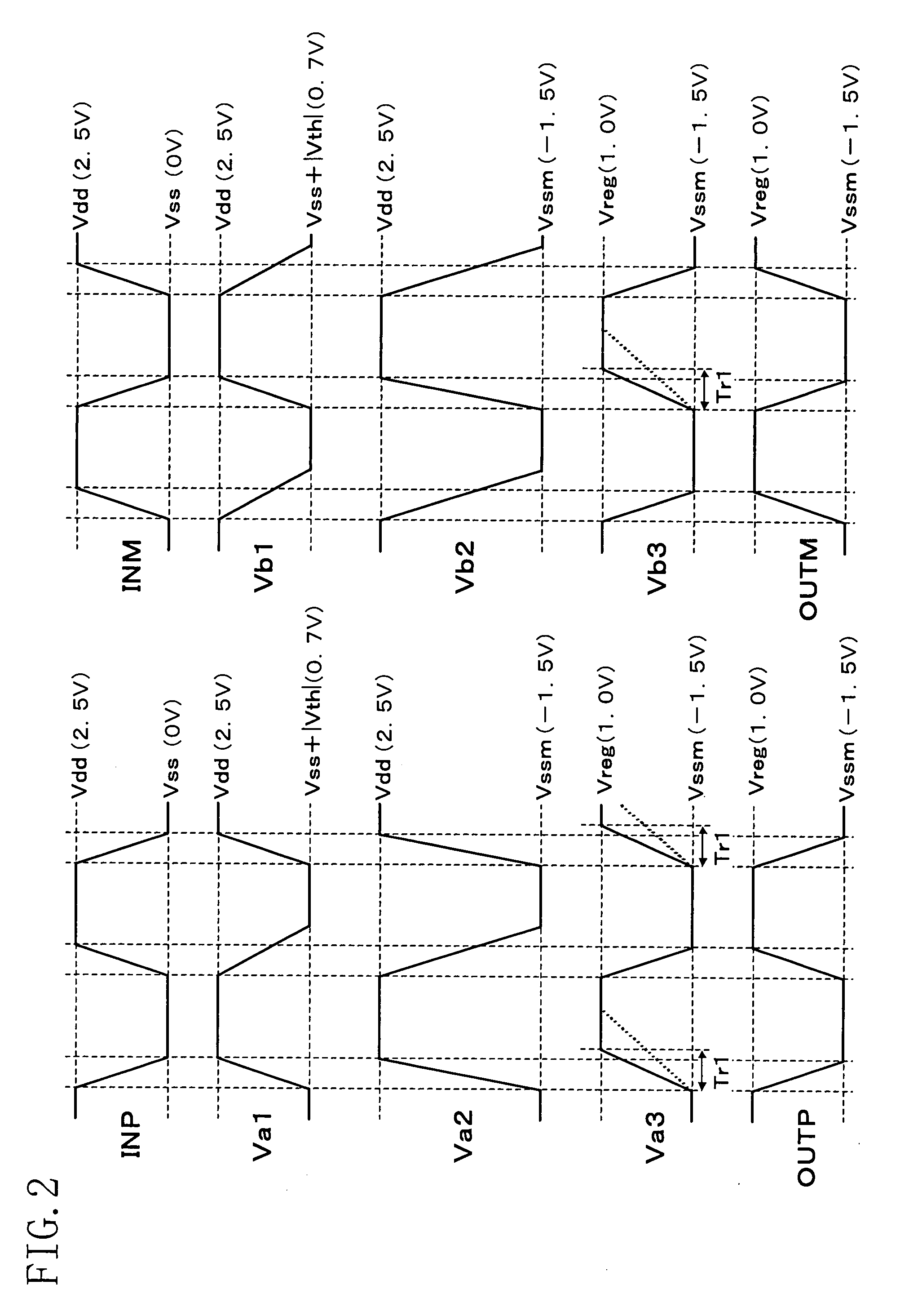
[0044]As shown in FIG. 3, if the transistors of FIG. 1 are arranged so that the polarities thereof are inverted and voltages Vss (0 [V]), Vdd1 (1 [V]), Vdd2 (2 [V]), Vdd2 (2 [V]) and Vdd3 (3 [V]) are applied to the reference nodes N1 to N5, it is possible to shift the input signals INP and INM having a level varying between the positive level “Vdd1” and the ground level “Vss” to a pair of output signals (OUTP, OUTM) having a level varying between the positive level “Vdd3” and the positive level “Vdd2”. Thus, it is possible to output a pair of output signals having a level varying between a positive level and a positive level.
second embodiment
[0045]FIG. 4 shows a configuration of a level shifter according to a second embodiment of the present invention. This level shifter comprises, in addition to the parts of FIG. 1, auxiliary transistors 201A and 201B and capacitance elements (capacitance sections) 202A and 202B. The gate of the auxiliary transistor 201A is connected to the gate of the input transistor 101A (the input signal INP is input thereto), the source thereof is connected to the reference node N2, and the drain thereof is connected to the source of the voltage relaxing transistor 102A. The auxiliary transistor 201B has a similar configuration. The capacitance element 202A is connected between the source and drain of the voltage relaxing transistor 103A. The capacitance element 202B has a similar configuration.
[0046]Next, an operation by the auxiliary transistors 201A and 201B of FIG. 4 and an operation by the capacitance elements 202A and 202B of FIG. 4 will be described with reference to FIG. 5.
[0047][Auxiliary...
third embodiment
[0059]FIG. 7 shows a configuration of a level shifter according to a third embodiment according to the present invention. This level shifter comprises, in addition to the parts of FIG. 1, a reset circuit 301 and an inverter circuit 302.
[0060]The reset circuit (signal supplying section) 301 receives a reference signal IN and a reset signal RESET, and when the reset signal RESET is at the “L level”, supplies the reference signal IN as the input signal INP to the gate of the input transistor 101A. The reference signal IN and the reset signal RESET are each, for example, a signal having a level varying between a positive level (Vdd) and a ground level (Vss). On the other hand, when the reset signal RESET is at the “H level”, the reset circuit 301 supplies the “H level” input signal INP to the input transistor 101A without depending on the logic level of the reference signal IN (i.e., the voltage level of the reference signal IN is forcedly fixed to the “H level”).
[0061]The inverter circ...
PUM
 Abstract
Description
Claims
Application Information