Apparatus for improving uniformity of luminosity in flat panel display

a technology of flat panel display and uniformity, applied in the direction of electric variable regulation, process and machine control, instruments, etc., can solve the problems of non-uniformity of luminance in the display area, failure to maintain upper and lower symmetry, left and right symmetry, and failure to minimize overall electrical resistan

Active Publication Date: 2009-08-25
SAMSUNG DISPLAY CO LTD
View PDF4 Cites 1 Cited by
  • Summary
  • Abstract
  • Description
  • Claims
  • Application Information

AI Technical Summary

Benefits of technology

[0016]The invention is directed to a flat panel display having an enhanced uniformity of luminance. In one embodiment, this is accomplished by incorporating in the flat panel display a supply line assembly configured to provide a uniform impedance.

Problems solved by technology

Such a configuration fails to maintain upper and lower symmetry and left and right symmetry or to minimize overall electrical resistance.
The problem most associated with configuring an anode wiring 130 in the conventional manner is that anode electrode line assembly 131 has an asymmetrical current distribution, which creates a non-uniformity of luminance in the display area 110.

Method used


Image

  • Apparatus for improving uniformity of luminosity in flat panel display
  • Apparatus for improving uniformity of luminosity in flat panel display
  • Apparatus for improving uniformity of luminosity in flat panel display

Examples


first embodiment

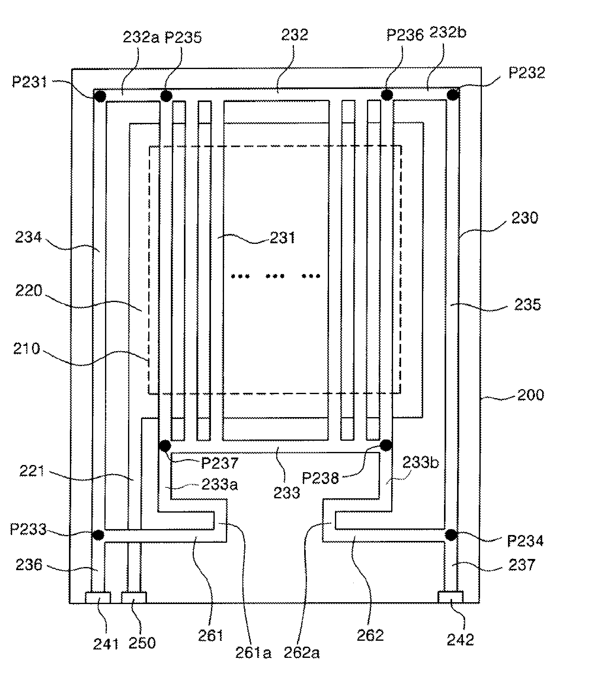
[0054]FIG. 6 is a top view of an anode wiring assembly 330 used in an OLED, and configured according to another embodiment of the invention. As shown, the anode wiring assembly 230 is substantially similar to that of the For example, the wiring assembly 330 of this embodiment is configured so that the current delivered through supply lines 336 and 337 from terminals 341 and 342 flows to an arbitrary anode electrode line of the plurality of anode electrode lines 331 arranged in a display area 310.

[0055]The anode wiring assembly 330 further includes a pair of first supply lines 361 and 362 and a pair of second supply lines 363 and 364 for impedance adjustment. Thus, the current supply line 330 is configured so that: (i) the impedance from the terminal 341 to the point P335 via the supply lines 336, 334 and 363 is the same as the impedance from the terminal 341 to the point P337 via the supply lines 336 and 361; and (ii) the impedance from the terminal 342 to the point P336 via the su...

third embodiment

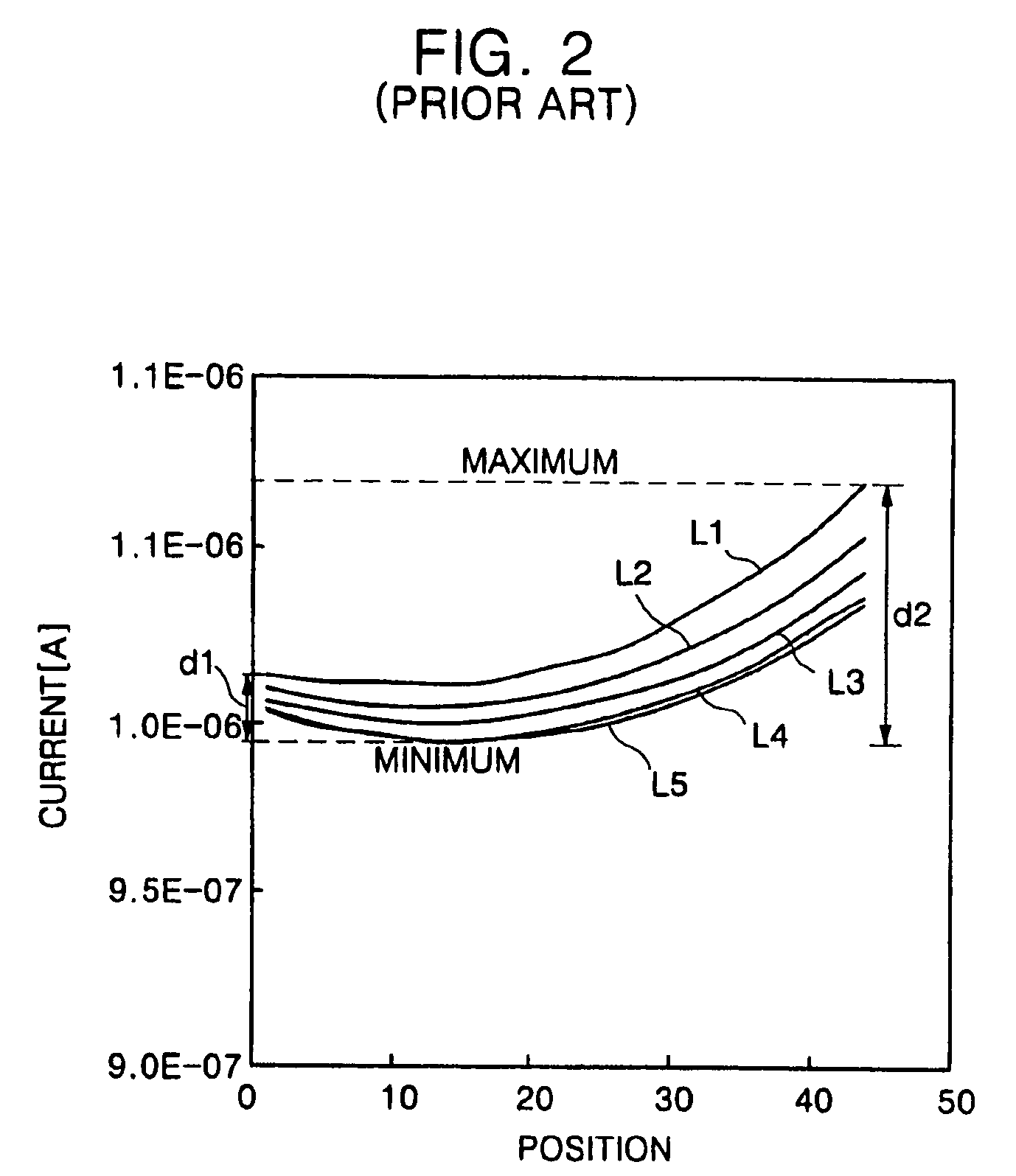
[0069]FIG. 8 is a chart illustrating current distribution in anode electrode lines of the anode wiring assembly 430 according to the invention. Referring to FIG.8, a difference d5 between minimum and maximum current values of the anode electrode lines L1 to L5 at the position X1 and a difference d6 between minimum and maximum current values of the anode electrode lines L1 to L5 at the position X44 are substantially similar and preferably identical to each other. Further, an inflection point of the current distribution curve, which is a point where a current value of each of the anode electrode lines L1 to L5 is minimized, is present between a position P1 / 4 and a position P3 / 4 of each of the anode electrode lines L1 to L5, and is preferably close to the position P1 / 2.

[0070]In addition, referring to FIG. 8, it is seen that a difference between the difference d5 between the minimum and maximum current values of the anode electrode lines L1 to L5 and the difference d6 between the minimu...


PUM


Abstract

A flat panel display includes a plurality of pixel anode electrodes arranged in a display area. A plurality of anode electrode lines for supplying a driving current to the pixel anode electrodes are connected at one end to pixel anode electrodes, and at the other to one or more current supply lines of a current supply line assembly. The current supply lines, in turn, are connected to first and second terminals to which the driving current is applied. The current supply line assembly also includes an impedance adjusting means for adjusting impedance of at least one of the first and second supply lines. The impedance adjusting means may be configured as a third separate supply line connected to at least one of the first and second supply lines, and the impedance of the current supply line is adjusted by varying the length or width of the third current supply line.

Description

CROSS-REFERENCE TO RELATED APPLICATION[0001]This application claims priority of Korean Patent Application No. 2003-56270, filed Aug. 13, 2003, which is herein incorporated by reference.BACKGROUND OF THE INVENTION[0002]The invention is directed to flat panel displays generally. More particularly, the invention is directed to an improved current supply line assembly having a uniform impedance, which is used in a flat panel display to improve the display's uniformity of luminance.[0003]An active matrix organic light-emitting display (AMOLED) includes a plurality of electroluminescent (EL) elements. Each EL element has R, G and B organic emission layers interposed between an anode electrode and a cathode electrode. Each R, G and B emission layer emits light when a first voltage is applied to the anode electrode and a second different voltage is applied to the cathode electrode.[0004]The anode electrodes are formed to be separated from one another in respective R, G and B unit pixels, bu...

Claims


Application Information

Patent Timeline
Patent Type & Authority Patents(United States)
IPC IPC(8): G06F3/038G09G3/20G09G3/30G09G5/10H02M3/335
CPCG09G3/3233G09G2320/0233G09G2300/0426G09G3/30
Inventor LEE, JUNG-WONHIROSHI, MIYAZAWAYOU, SUK-BEOM
Owner SAMSUNG DISPLAY CO LTD
Why Eureka
Try Eureka