Semiconductor device, display device and method for manufacturing thereof, and television device

a technology of semiconductor devices and display devices, which is applied in the direction of discharge tubes/lamp details, discharge tubes luminescnet screens, electric discharge lamps, etc., can solve the problems of increasing the number of photolithography steps, and the manufacturing cost is inevitable to increase, so as to achieve good adhesiveness, reduce material loss and cost, and high performance

Inactive Publication Date: 2009-09-01
SEMICON ENERGY LAB CO LTD
View PDF18 Cites 65 Cited by
  • Summary
  • Abstract
  • Description
  • Claims
  • Application Information

AI Technical Summary

Benefits of technology

[0006]It is an object of the present invention to provide a technique for manufacturing a TFT, an electronic circuit using the TFT and a display device formed using the TFT, even over a large substrate having 1 m or more on a side at low cost and with high yield by reducing the number of photolithography steps and simplifying the manufacturing process.
[0007]Further, another object of the invention is to provide a technique for forming a component such as a wiring constituting a part of such a semiconductor device and a display device to have a desired shape with good adhesiveness.
[0008]In the present invention, the adhesiveness between a first conductive layer and a second conductive layer is increased by forming a buffer layer including at least one pore between them. A pore contained in the buffer layer including at least one pore is filled with a particle shaped conductive material, and is solidified by baking, and then a second conductive layer is formed. The second conductive layer is formed with good adhesiveness and stability with the first conductive layer by anchoring effect (also referred to as anchor effect), in which the conductive layer solidified in the pore has a function like a needle or a wedge.
[0030]The present invention enables conductive films to be formed with good adhesiveness to each other. In addition, material loss and costs can be reduced. Therefore, a semiconductor device and a display device having high performance and high reliability can be manufactured with high yield.

Problems solved by technology

Therefore, the manufacturing cost is inevitably increased with the increase of the number of photolithography steps.

Method used


Image

  • Semiconductor device, display device and method for manufacturing thereof, and television device
  • Semiconductor device, display device and method for manufacturing thereof, and television device
  • Semiconductor device, display device and method for manufacturing thereof, and television device

Examples


embodiment mode 1

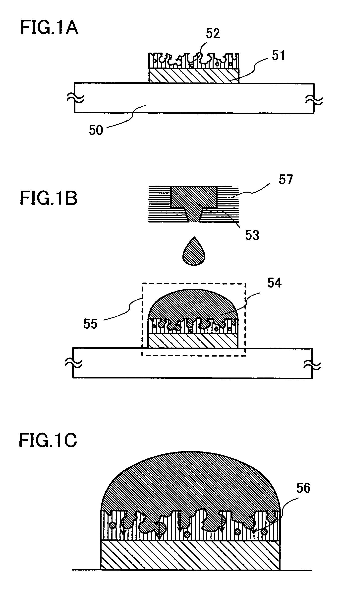
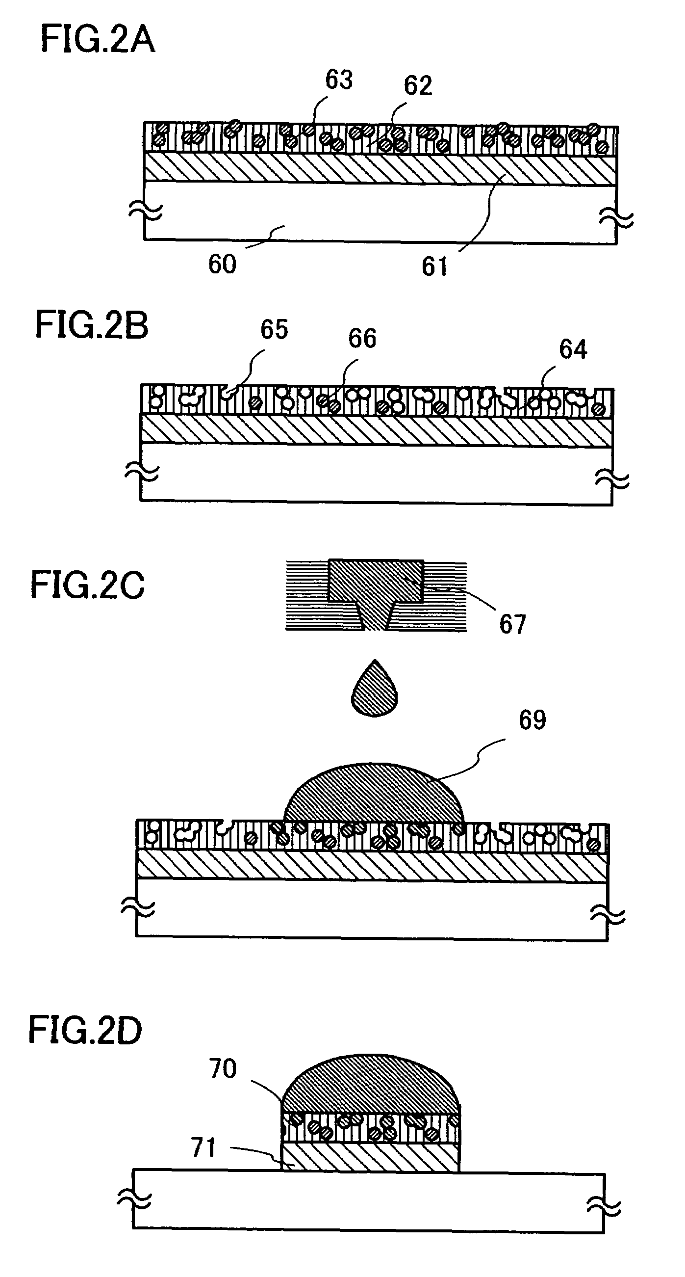
[0062]Embodiment Mode of the present invention will be described with reference to FIGS. 1A to 1C and FIGS. 2A to 2D.

[0063]The characteristic of the present invention is that, to manufacture a semiconductor device or a display device, at least one or more of the components necessary for manufacturing the semiconductor device or the display device, such as a conductive layer forming a wiring layer or an electrode, and a mask layer for forming a predetermined pattern, is formed by a method in which such components can be selectively formed in a desired shape. In the present invention, a component (also referred to as a pattern) means a conductive layer such as a wiring layer, a gate electrode layer, a source electrode layer, a drain electrode layer; a semiconductor layer; a mask layer; an insulating layer, and the like constituting a thin film transistor or a display device, and all component elements formed in a predetermined shape are included. As a method for forming a formation in...

embodiment mode 2

[0095]FIG. 25A is a top view showing a structure of a display panel according to the present invention, wherein a pixel portion 2701 in which pixels 2702 are arranged in matrix form, a scanning line input terminal 2703, and a signal line input terminal 2704 are formed over a substrate 2700 having an insulated surface. The number of pixels may be determined in accordance with various standards. The number of pixels for XGA for full color display using RGB may be 1,024×768×3 (RGB), and that for UXGA for full color display using RGB may be 1,600×1,200×3 (RGB). In a case of forming a display panel corresponding to a full-spec high vision for full color display using RGB, the number of pixels may be 1,920×1,080×3 (RGB).

[0096]The pixels 2702 are arranged in matrix form by intersecting scanning lines extending from the scanning line input terminal 2703 with signal lines extending from the signal line input terminal 2704. Each pixel 2702 includes a switching element and a pixel electrode co...

embodiment mode 3

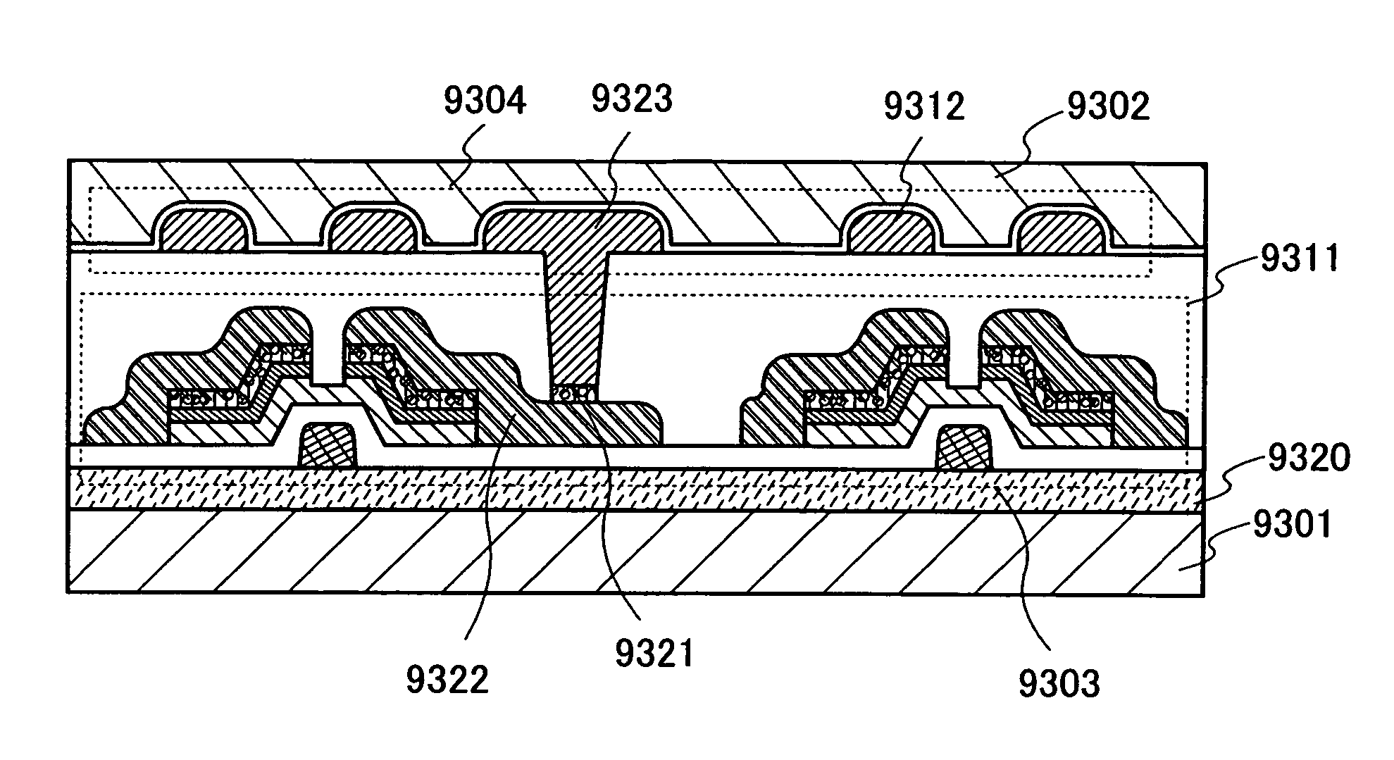
[0155]Embodiment Modes of the present invention will be described with reference to FIGS. 11 to 13. The details thereof will be described using a method for manufacturing a display device having a thin film transistor of a top gate planar structure obtained by applying the present invention. FIG. 12A is a top view of a pixel portion of the display device. FIGS. 11A to 11D and 12B are cross-sectional views of the pixel portion of the display device taken along line E-F in each process. FIG. 13A is also a top view of the display device, and FIG. 13B is a cross-sectional view taken along line O-P (including U-W) of FIG. 13A. An example of a liquid crystal display device using a liquid crystal material as a display element is shown. Therefore, a description of the same part or a part having a similar function will be omitted.

[0156]Over a substrate 200 having an insulated surface, a base film 201a is formed using a silicon nitride oxide (SiNO) film to have a film thickness of 10 to 200 n...


PUM


Abstract

The purpose of the present invention is to provide a semiconductor device or a display device that can be manufactured by improving the use efficiency of a material as well as simplifying the manufacturing process, and a manufacturing technique of those devices. Also, another purpose of the present invention is to provide a technique for forming a pattern of wirings, etc., constituting the semiconductor device or the display device, in a desired shape and with good adhesiveness. The adhesiveness between first and second conductive layers is increased by forming a conductive buffer layer including at least one pore between them. The second conductive layer is formed by filling the pores of the buffer layer including at least one pore with a particle shaped conductive material which is solidified by baking. The conductive layer solidified in the pores functions like a wedge, and the second conductive layer is formed over the first conductive layer with good adhesiveness and stability.

Description

BACKGROUND OF THE INVENTION[0001]1. Field of Invention[0002]The present invention relates to a semiconductor device, a display device and a method for manufacturing thereof, and a television device.[0003]2. Description of the Related Art[0004]A thin film transistor (hereinafter also referred to as a “TFT”) and an electric circuit using the thin film transistor are formed by stacking various kinds of thin films such as a semiconductor, an insulator and a conductor over a substrate, and appropriately patterning into a predetermined shape using photolithography technique. Photolithography technique is a technique in which a pattern of a circuit or the like, which is formed on a transparent plane plate called a photomask using a non-light-transmitting material, is transferred to an intended substrate by utilizing light. The photolithography technique is widely used in a process of manufacturing a semiconductor integrated circuit, and the like.[0005]The conventional manufacturing process...

Claims


Application Information

Patent Timeline
Patent Type & Authority Patents(United States)
IPC IPC(8): H01L33/00
CPCH01L29/458H01L29/4908H01L27/1292H01L2924/0002H01L2924/00
Inventor FUJII, GENMORISUE, MASAFUMI
Owner SEMICON ENERGY LAB CO LTD
Why Eureka
Try Eureka