Image sensors including impurity layer adjacent isolation region

a technology of image sensors and impurity layers, applied in the direction of electrical equipment, semiconductor devices, radio frequency controlled devices, etc., can solve the problems of image sensors suffering from a phenomenon known as “dark current, dark current, damage to sti trench walls, etc., and achieve the effect of rapid thermal annealing and reduced dark curren

Active Publication Date: 2009-09-08
SAMSUNG ELECTRONICS CO LTD
View PDF15 Cites 6 Cited by
  • Summary
  • Abstract
  • Description
  • Claims
  • Application Information

AI Technical Summary

Benefits of technology

[0020]Integrated circuits may be fabricated, according to some embodiments of the present invention, by etching a plurality of spaced apart isolation trenches in an integrated circuit substrate, the trenches including trench walls. A sacrificial layer, including an impurity therein, is formed on at least some of the trench walls. At least some of the impurity is diffused from the sacrificial layer into the trench walls to form an impurity layer in the substrate adjacent the trench walls. In some embodiments, the diffusion may take place by rapid thermal annealing. At least some of the sacrificial layer is then removed. In still other embodiments, after the sacrificial layer has been at least partially removed, an insulating layer may be formed in the trenches. In other embodiments, the trenches may be filled with insulating material, to form isolation regions. In some embodiments, a plurality of photoelectric conversion elements is also formed in the substrate, such that the photoelectric elements are adjacent the impurity layer, and the impurity layer reduces dark current in the photoelectric conversion elements compared to absence of the impurity layer.

Problems solved by technology

As is also well known to those having skill in the art, image sensors may suffer from a phenomenon known as “dark current”.
As is also well known to those having skill in the art, dark current may be caused by silicon dangling bonds, plasma damage, stress, implant damage, wafer defects, undesired electric fields and / or many other phenomena that may arise in the fabrication of an image sensor.
In particular, it is known that the STI trench walls may have damage that is caused by anisotropic etching or dry etching processes that are used in fabricating the trenches.
Etching damage, such as dangling bonds and / or stacking faults, may contribute to dark current.

Method used


Image

  • Image sensors including impurity layer adjacent isolation region
  • Image sensors including impurity layer adjacent isolation region
  • Image sensors including impurity layer adjacent isolation region

Examples


Embodiment Construction

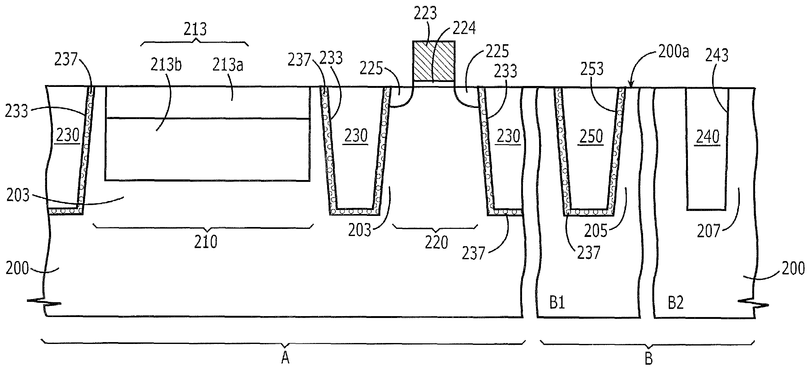
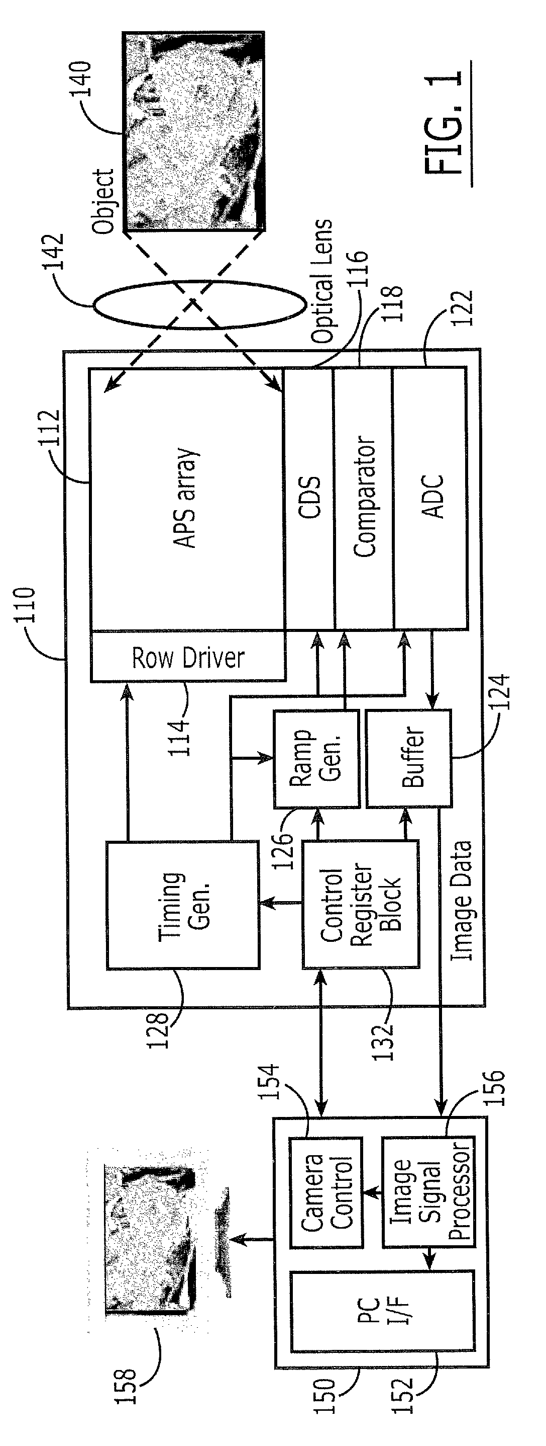
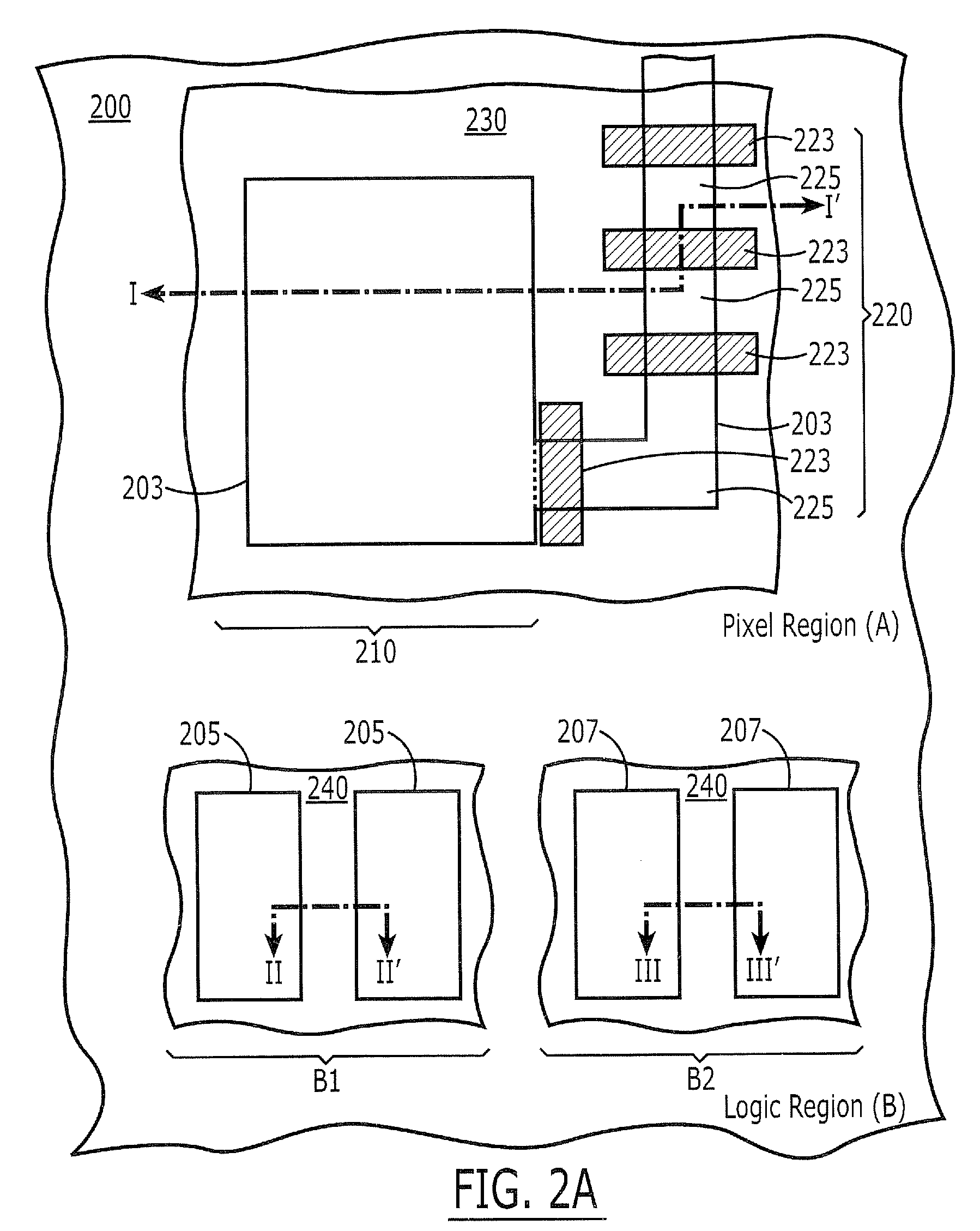
[0035]The invention will be described more fully hereinafter with reference to the accompanying drawings, in which example embodiments of the invention are shown. This invention may, however, be embodied in many different forms and should not be construed as limited to the example embodiments set forth herein. Rather, the disclosed embodiments are provided so that this disclosure will be thorough and complete, and will fully convey the scope of the invention to those skilled in the art. In the drawings, the size and relative sizes of layers and regions may be exaggerated for clarity. Moreover, each embodiment described and illustrated herein includes its complementary conductivity type embodiment as well. Like numbers refer to like elements throughout.

[0036]It will be understood that when an element or layer is referred to as being “on”, “connected to” and / or “coupled to” another element or layer, it can be directly on, connected or coupled to the other element or layer or interveni...


PUM


Abstract

Image sensors include a pixel region and a logic region. Pixel isolation regions in the pixel region include pixel isolation region walls that are less sloped than logic isolation region walls in the logic region. An impurity layer also may be provided adjacent at least some of the pixel isolation region walls, wherein at least some of the logic isolation region walls are free of the impurity layer. The impurity layer and / or the less sloped logic isolation region walls may also be provided for NMOS devices in the logic region but not for PMOS devices in the logic region. Doped sacrificial layers may be used to fabricate the impurity layer.

Description

CROSS REFERENCE TO RELATED APPLICATION[0001]This application claims the benefit under 35 USC §119 of Korean Patent Application No. 10-2006-0075705, filed on Aug. 10, 2006, the disclosure of which is hereby incorporated herein by reference in its entirety as if set forth fully herein.FIELD OF THE INVENTION[0002]This invention relates to integrated circuit devices and related fabrication methods, and more particularly to image sensor integrated circuit devices and fabrication methods therefor.BACKGROUND OF THE INVENTION[0003]Integrated circuit image sensors are widely used for capturing images in a variety of applications, such as digital cameras, camcorders, printers, scanners, etc. Integrated circuit image sensors generally include a plurality of photoelectric conversion elements that capture optical information and convert the optical information into electrical signals. A plurality of logic circuits is also included, which can be used to control the photoelectric conversion elemen...

Claims


Application Information

Patent Timeline
Patent Type & Authority Patents(United States)
IPC IPC(8): H01L31/00H01L31/062
CPCH01L27/14603H01L27/14689H01L27/1463H01L27/14609H01L27/146
Inventor KWON, DOOWONSHIN, SEUNG-HUN
Owner SAMSUNG ELECTRONICS CO LTD
Why Eureka
Try Eureka