Piezoelectric material and piezoelectric device

a piezoelectric device and piezoelectric technology, applied in the field of piezoelectric materials and piezoelectric devices, can solve problems such as serious environmental problems, and achieve the effect of excellent piezoelectric characteristics

Active Publication Date: 2009-09-08
SEIKO EPSON CORP
View PDF11 Cites 23 Cited by
  • Summary
  • Abstract
  • Description
  • Claims
  • Application Information

AI Technical Summary

Benefits of technology

[0006]In accordance with an aspect of the present invention, there is provided a novel piezoelectric material that is environmental-friendly and has excellent piezoelectric characteristics, and a piezoelectric device having a piezoelectric layer composed of the piezoelectric material.
[0009]The piezoelectric material described above does not contain lead (Pb) that poses an environmental problem, and therefore is very useful. Further, the piezoelectric material is free of lead, but has excellent piezoelectric characteristics, whereby, for example, a sufficient amount of lattice distortion can be obtained.

Problems solved by technology

However, PZT includes lead (Pb), and this may pose a serious environmental problem.

Method used


Image

  • Piezoelectric material and piezoelectric device
  • Piezoelectric material and piezoelectric device

Examples


first embodiment

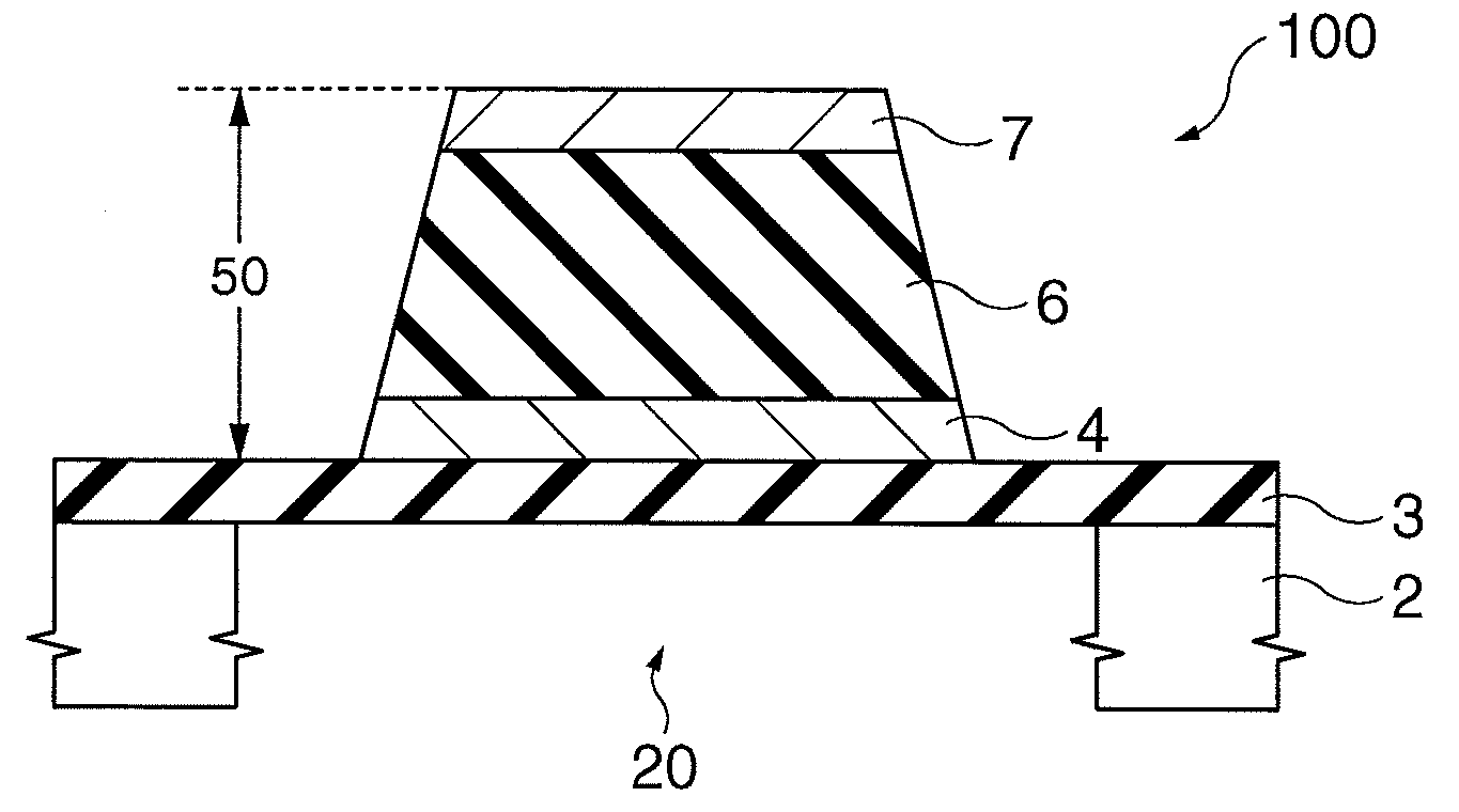
[0044]2.2. Next, a method for manufacturing the piezoelectric device 100 in accordance with the first embodiment is described with reference to FIG. 1.

[0045](A) First, an elastic layer 3 is formed on a base substrate 2. The elastic layer 3 may be formed by, for example, a thermal oxidation method, a chemical vapor deposition (CVD) method, a sputter method, or a vapor deposition method.

[0046](B) Then, a lower electrode 4 is formed on the elastic layer 3. The lower electrode 4 may be formed by, for example, a sputter method, a spin coat method, a CVD method, or a laser ablation method.

[0047](C) Next, a piezoelectric layer 6 composed of the piezoelectric material in accordance with the present embodiment is formed on the lower electrode 4. The piezoelectric layer 6 may be formed by using, for example, a sol-gel method, or a MOD (metal organic decomposition) method. In accordance with a concrete example, the method for forming the piezoelectric layer 6 by using a sol-gel method or a MOD...

second embodiment

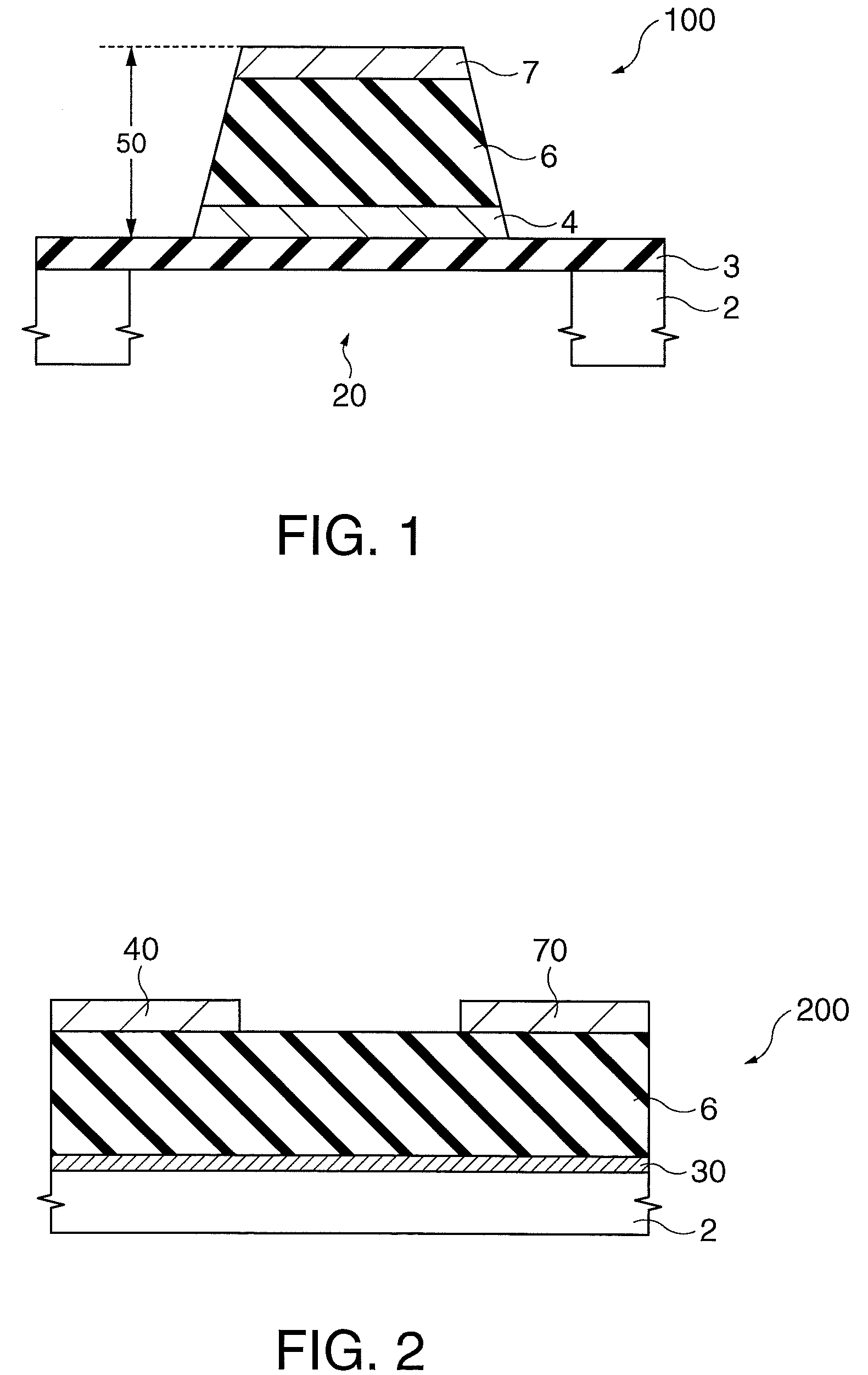
[0079]3.2. Next, a method for manufacturing the piezoelectric device 200 in accordance with the second embodiment is described with reference to FIG. 2.

[0080](A) First, a buffer layer 30 is formed on a base substrate 2. The buffer layer 30 may be formed by, for example, a sputter method, a spin coat method, a CVD method, or a laser ablation method.

[0081](B) Then, a piezoelectric layer 6 is formed on the buffer layer 30. This process is substantially the same as the process of manufacturing the piezoelectric device 100 of the first embodiment described above, and therefore its detailed description is omitted.

[0082](C) Next, a first electrode 40 and a second electrode 70 are formed on the piezoelectric layer 6. The first electrode 40 and the second electrode 70 may be formed by, for example, a sputter method, a spin coat method, a CVD method, or a laser ablation method. The first electrode 40 and the second electrode 70 may be patterned by a known method.

[0083](D) Then, post annealing...


PUM

PropertyMeasurementUnit
angleaaaaaaaaaa
thicknessaaaaaaaaaa
temperatureaaaaaaaaaa

Abstract

A piezoelectric material is expressed by a general formula (1) as follows: (Bi1−xBax)(Fe1−xTix)O3 . . . (1), where x is greater than 0, but smaller than 1 (0<x<1).

Description

[0001]The entire disclosure of Japanese Patent Application No. 2006-110033, filed Apr. 12, 2006 is expressly incorporated by reference herein.BACKGROUND[0002]1. Technical Field[0003]The present invention relates to piezoelectric material and piezoelectric devices.[0004]2. Related Art[0005]Piezoelectric devices used for heads of ink jet printers have piezoelectric layers composed of piezoelectric material. Pb(Zr, Ti)O3(PZT) is a representative material as the piezoelectric material. For example, an example of related art is described in Japanese Laid-open patent application JP-A-2001-223404. However, PZT includes lead (Pb), and this may pose a serious environmental problem.SUMMARY[0006]In accordance with an aspect of the present invention, there is provided a novel piezoelectric material that is environmental-friendly and has excellent piezoelectric characteristics, and a piezoelectric device having a piezoelectric layer composed of the piezoelectric material.[0007]A piezoelectric ma...

Claims


Application Information

Patent Timeline
Patent Type & Authority Patents(United States)
IPC IPC(8): H01L41/08B41J2/075B41J2/14C04B35/00C04B35/462H01L41/09H01L41/18H01L41/187H01L41/22H01L41/319
CPCH01L41/0973H01L41/1878H01L41/0815H01L41/318H10N30/10516H10N30/2047H10N30/8561H10N30/078
Inventor MIYAZAWA, HIROMUHAMADA, MAYUMI
Owner SEIKO EPSON CORP
Why Eureka
Try Eureka