Trimming circuit and semiconductor device
a technology of zener diodes and circuits, applied in the field of zener diodes, can solve the problems of zener diodes being broken, increasing the area of terminals, and increasing the cost of ic chips
- Summary
- Abstract
- Description
- Claims
- Application Information
AI Technical Summary
Benefits of technology
Problems solved by technology
Method used
Image

Examples
first embodiment
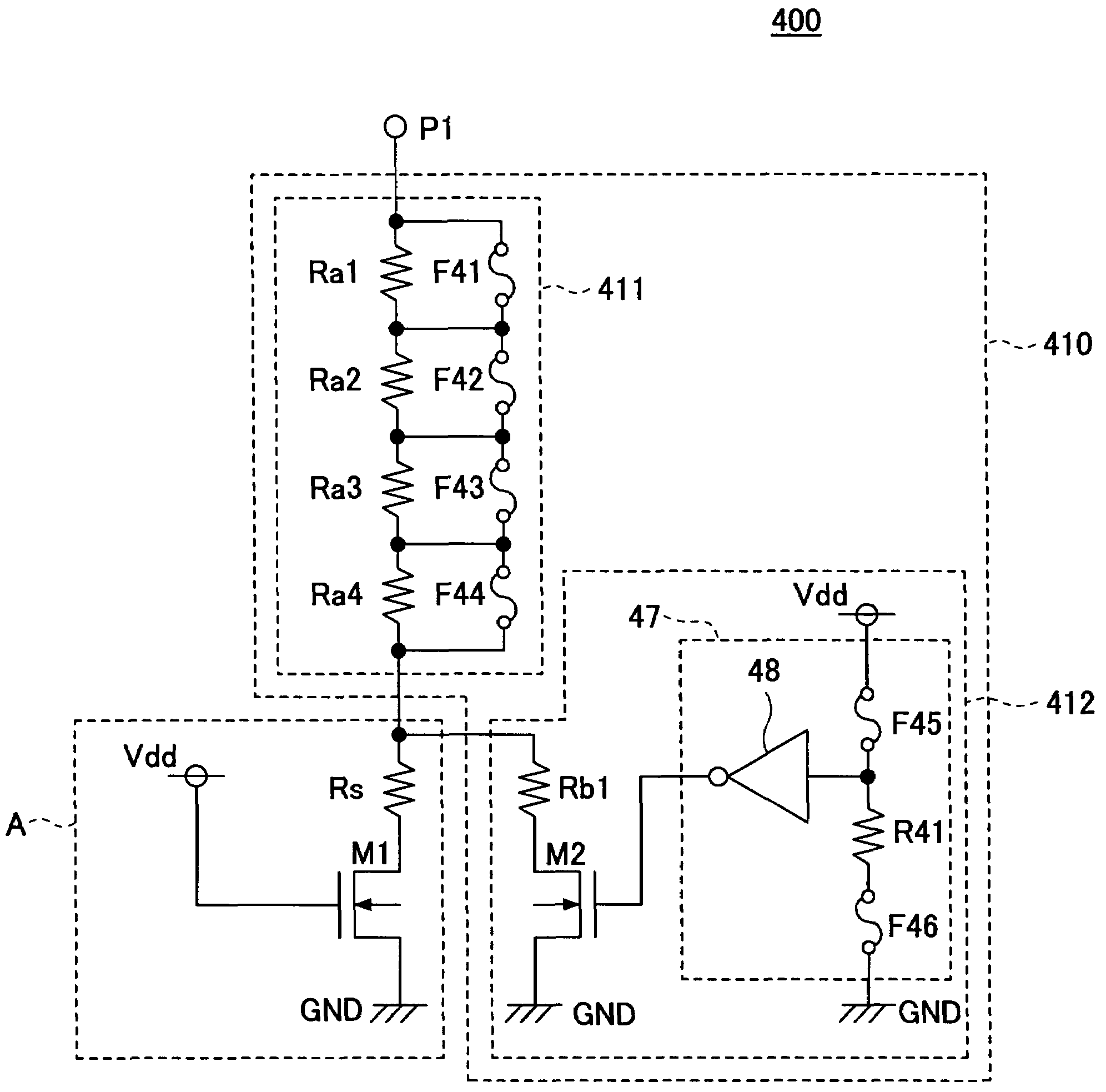
[0037]Referring to the drawing, a first embodiment of the present invention is described. FIG. 4 is a circuit diagram of a semiconductor device 400 having a trimming circuit 410 according to the first embodiment of the present invention.
[0038]As shown in FIG. 4, the semiconductor device 400 includes the trimming circuit 410 and a reference resistor section A connected to the trimming circuit 410. The trimming circuit 410 and the reference resistor section A are connected between a terminal P1 and a ground terminal GND. In the semiconductor device 400, a combined resistance value R between the terminal P1 and the ground terminal GND is adjusted to a target resistance value Rd in the trimming circuit 410. The combined resistance value R is used for a circuit (not shown) connected to the terminal P1. The target resistance value Rd is predetermined when designing a circuit in an IC chip corresponding to, for example, characteristics of the IC chip.
[0039]First, the reference resistor sec...
second embodiment
[0096]Referring to the drawing, a second embodiment of the present invention is described. FIG. 5 is a circuit diagram of a semiconductor device 400A having a trimming circuit 410A according to the second embodiment of the present invention.
[0097]As shown in FIG. 5, in the trimming circuit 410A, the second trimming circuit 412 described in the first embodiment is replaced by a second trimming circuit 412A. Other sections are the same as those described in the first embodiment of the present invention. Therefore, in the second embodiment of the present invention, only the difference from the first embodiment of the present invention is described and the description of the same sections as those in the first embodiment of the present invention is omitted.
[0098]The second trimming circuit 412A is connected to the reference resistor section A in parallel and includes resistors Rb1 and Rb2, NMOS transistors M2 and M3, and control circuits 51 and 52.
[0099]The resistor Rb1 and the NMOS tra...
third embodiment
[0143]Referring to the drawing, a third embodiment of the present invention is described. FIG. 6 is a circuit diagram of a semiconductor device 600 having the trimming circuit 410 according to the third embodiment of the present invention. The semiconductor device 600 according to the third embodiment of the present invention is a constant-current circuit including the trimming circuit 410 and the reference resistor section A described in the first embodiment of the present invention. Therefore, the description of the trimming circuit 410 and the reference resistor section A is omitted.
[0144]The semiconductor device 600 of the constant-current circuit includes a reference voltage Vref, an operational amplifier (AMP) 62, an NMOS transistor M4, the trimming circuit 410, and the reference resistor section A.
[0145]The reference voltage Vref is applied to the non-inverting input terminal of the AMP 62, and the inverting input terminal of the AMP 62 is connected to the terminal P1 of the ...
PUM
 Abstract
Description
Claims
Application Information
 - R&D Engineer
- R&D Manager
- IP Professional
- Industry Leading Data Capabilities
- Powerful AI technology
- Patent DNA Extraction
Browse by: Latest US Patents, China's latest patents, Technical Efficacy Thesaurus, Application Domain, Technology Topic.
© 2024 PatSnap. All rights reserved.Legal|Privacy policy|Modern Slavery Act Transparency Statement|Sitemap