Cantilever-type probe card for high frequency application

a probe card and high frequency technology, applied in the field of probe cards, can solve the problems of lowering the reliability of the wafer level test and dielectric loss, and achieve the effect of high test reliability

Inactive Publication Date: 2009-09-29
MPI CORP
View PDF11 Cites 23 Cited by
  • Summary
  • Abstract
  • Description
  • Claims
  • Application Information

AI Technical Summary

Benefits of technology

[0009]The present invention has been accomplished under the circumstances in view. It is therefore the main object of the present invention to provide a cantilever-type probe card, which achieves high quality transmission of high frequency test signal, and is effective for use in a wafer level test work.
[0011]When the signal probes and the at least one grounding probe probing on the ICs of the test wafer, there is a longitudinal buffer for each of the probing tips to maintain optimal contact with the ICs of the test wafer and to buffer the stress acted upon the probes as the probing tips are receiving the anti-force reacted by the probed ICs. Further, because the front arms of the probes are suspended in the grounding block and kept spaced from the grounding block at a predetermined pitch, the desired characteristic impedance matching is well maintained for high frequency signal transmission, ensuring high test reliability.

Problems solved by technology

However, because the probes 13 are simply formed of a conducting metal without having a similar design functioned like the coaxial transmission lines 11, the parasitic capacitor that is induced subject to the dielectric surrounding around each of the probes 13 may cause the dielectric loss during a high frequency signaling through the probe 13, thus lowering the reliability of the wafer level test.

Method used


Image

  • Cantilever-type probe card for high frequency application
  • Cantilever-type probe card for high frequency application
  • Cantilever-type probe card for high frequency application

Examples


first embodiment

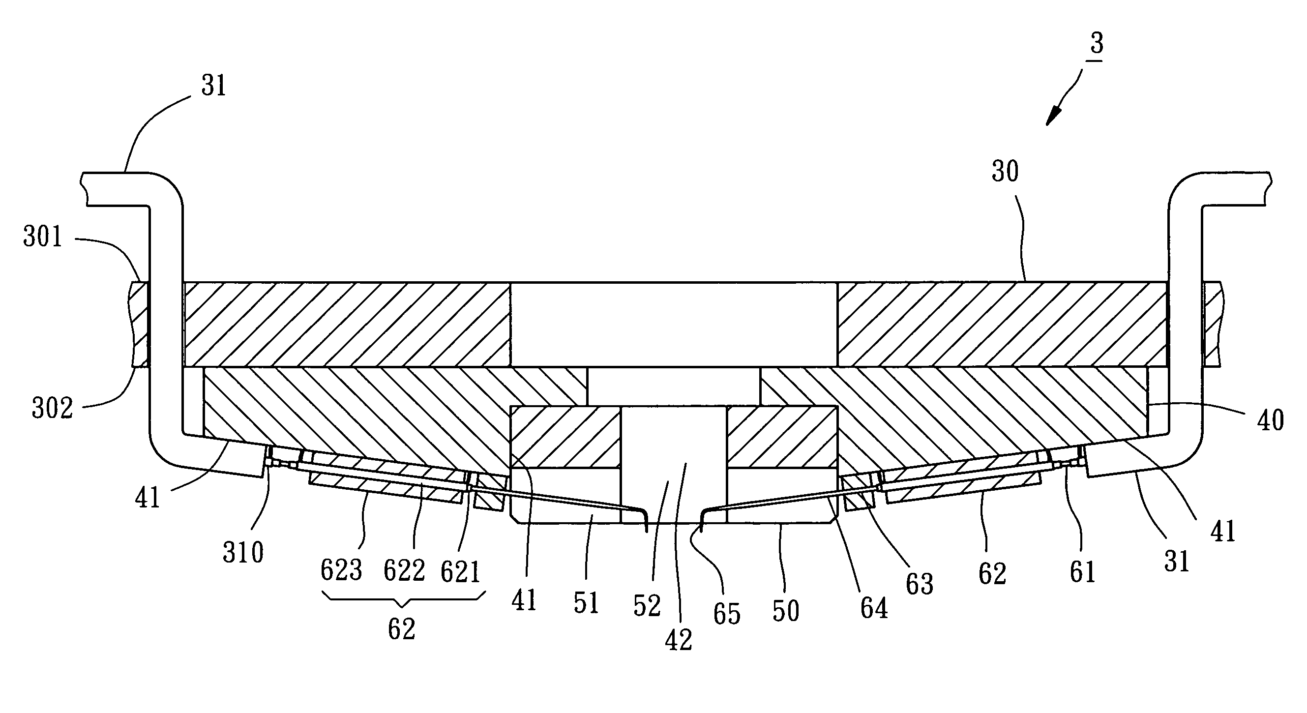
[0023]Referring to FIGS. 3-6, a cantilever-type probe card 3 for testing semiconductor wafers or the like in accordance with the present invention is shown comprised of a circuit board 30, a probe holder 40, a grounding block 50, a plurality of signal probes 60, and a plurality of grounding probes 70.

[0024]The circuit board 30 defines a top surface 301 and a bottom surface 302 opposite to the top surface 301. The top surface 301 is adapted to be electrically connected to a test machine (not shown), which is controllable to output high frequency test signals to the probe card 3. The circuit board 30 has arranged thereon electronic circuits, including multiple signal lines 31 and grounding lines 32. As shown in FIG. 3, the signal lines 31 are coaxial transmission lines for the transmission of high frequency signals, and extended from the top surface 301 to the bottom surface 302 and then respectively electrically connected to the signal probes 60. Further, each of the signal lines 31 ...

third embodiment

[0030]Further, the signal probes of a cantilever-type probe card in accordance with the present invention are not limited to the aforesaid coaxial probe structure. FIG. 10 shows a cantilever-type probe card 5 in accordance with the present invention for use in measure of LCD driver IC with high-frequency differential signaling. As illustrated, differential transmission lines 33 and differential probes 90 are used in this embodiment to substitute for the aforesaid signal lines 31 and signal probes 60. Each of the differential transmission lines 33 is a biaxial wiring structure, comprises dual wires surrounded coaxially by a metal shield 330 that is electrically connected to the probe holder 40. Each probe 90 comprises two bared needles 900 that are spaced from each other at a predetermined pitch and electrically connected to the associating differential transmission line 33, two dielectric layers 901 respectively surrounding the bared needles 900, a grounding layer 92 surrounding the...


PUM


Abstract

A cantilever-type probe card includes a circuit board, a grounding block electrically connected to a zero potential, signal probes, and at least one grounding probe connected to the grounding block. Each signal probe has a probing tip, a connection portion affixed to the circuit board, and a front arm defined between the connection portion and the probing tip. The front arm of each of the signal probes is suspended in the grounding block and spaced from the grounding block at a predetermined pitch.

Description

BACKGROUND OF THE INVENTION[0001]1. Field of the Invention[0002]The present invention relates to probe cards and more particularly, to a cantilever-type probe card for high frequency application.[0003]2. Description of the Related Art[0004]FIG. 1 shows a cantilever-type probe card 1 according to the prior art. According to this design, the probe card 1 comprises a circuit board 10, a plurality of coaxial transmission lines 11, a probe holder 12, and a plurality of probes 13. The circuit board 10 has a plurality of contact pads 101 on the top side near the border for receiving test signals from a test machine. The coaxial transmission lines 11 are electrically connected between the contact pads 101 and the probes 13 for transmission of test signals from the test machine to the probes 13 which can electrically probe ICs of a semiconductor wafer.[0005]The probe holder 12 has a grounding plane 121, a holder body 122, and a plurality of fastening members 123. The grounding plane 121 is e...

Claims


Application Information

Patent Timeline
Patent Type & Authority Patents(United States)
IPC IPC(8): G01R31/02
CPCG01R1/07342G01R1/06772
Inventor KU, WEI-CHENGHO, CHIH-HAOLIN, SHU-KAN
Owner MPI CORP
Why Eureka
Try Eureka