Electronic component and method for manufacturing the same

a technology of electronic components and resistive films, applied in the field of electronic components, can solve the problems of insufficient space for electroconductive pastes applied by the second and subsequent screen printing, high cost of preparing the corresponding screen plate for each, and insufficient resistance of resistive film coatings, etc., to achieve stable resistance, reduce the variation in resistance of the resulting resistive film, and increase the mixing time of ink

Active Publication Date: 2009-09-29
MURATA MFG CO LTD
View PDF10 Cites 6 Cited by
  • Summary
  • Abstract
  • Description
  • Claims
  • Application Information

AI Technical Summary

Benefits of technology

[0013]Accordingly, the present disclosure provides an electronic component including a resistor element can be efficiently produced with a range of resistances, and a method for manufacturing the electronic component.

Problems solved by technology

Accordingly, a high cost is required for preparing a corresponding screen plate for each resistance and it takes a long time to prepare the screen plates.
Furthermore, electroconductive pastes applied by the second and subsequent screen printing do not sufficiently fill the spaces between the previously printed electroconductive pastes, and gaps may be formed.
It is thus difficult to simplify the process.
This is not suitable for small-volume production in great varieties.

Method used


Image

  • Electronic component and method for manufacturing the same
  • Electronic component and method for manufacturing the same
  • Electronic component and method for manufacturing the same

Examples


embodiment 1

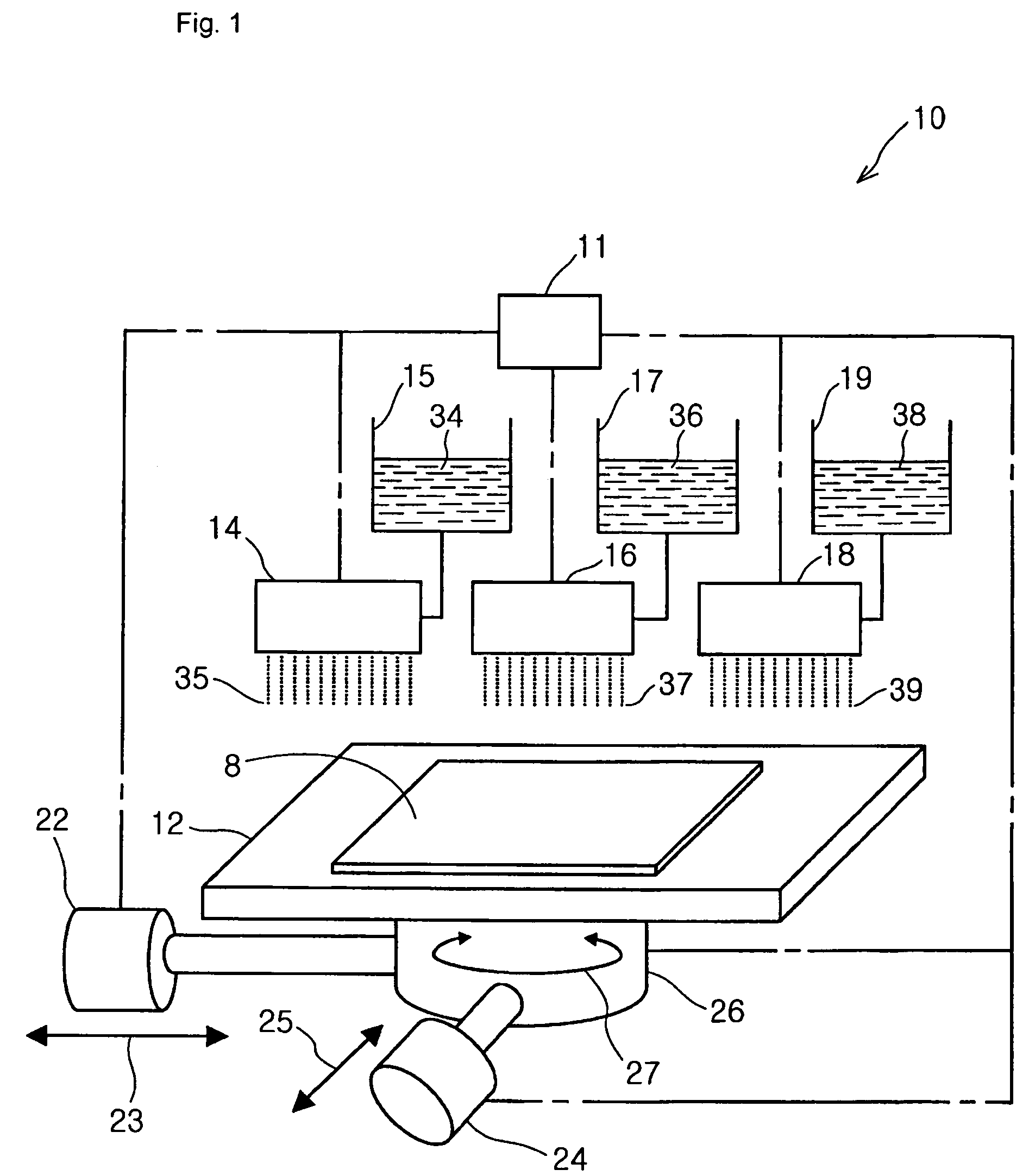
[0054]Embodiment 1 will now be described with reference to FIGS. 1 to 3.

[0055]An ink jet printer 10 used for printing a pattern intended for a resistive film (resistor element) will first be described with reference to the schematic representation shown in FIG. 1.

[0056]The ink jet printer 10 generally includes a movable table 12 on which a base material 8 is placed, a plurality of (for example, three) ink jet heads 14, 16, and 18, and a controller 11 controlling the entire apparatus.

[0057]The movable table 12 is driven in the X direction designated by reference numeral 23 by a motor 22, in the Y direction designated by reference numeral 25 by another motor 24, and in the θ direction designated by reference numeral 27 (around on the Z axis perpendicular to the x and the y axis) by still another motor 26. The drive of the movable table 12 by the motors 22, 24, and 26 is controlled by the controller 11. The movable table 12 may be able to move in a direction other than the X, Y, and θ ...

embodiment 2

[0090]Embodiment 2 will now be described with reference to FIGS. 4 and 5.

[0091]In Embodiment 2 as well, an ink jet printer is used for printing.

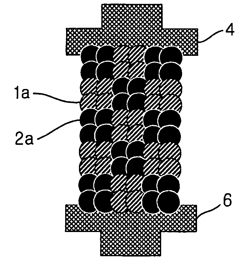
[0092]As schematically shown in FIG. 4, resistive inks ejected from the respective ink jet heads 14 and 16 are simultaneously printed at substantially the same position on a base material 8 disposed on a movable table 12. In this instance, some or all of the dots 1a of resistive ink 1 ejected from the ink jet head 14 and some or all of the dots 2a of resistive ink 2 ejected from the ink jet head 16 are disposed one on top of the other. Also, the dots 2a of resistive ink 2 are disposed on the dots 1a of resistive ink 1 before the dots 1a are dried so that the dots 1a and 2a of resistive inks 1 and 2 are mixed. In order to accelerate the mixing, supersonic waves may be applied. Part of the constituents of resistive ink 1 and part of the constituents of resistive ink 2 may chemically react with each other or form an alloy by the mixing.

[0093]Pr...

embodiment 3

[0103]Embodiment 3 will now be described with reference to FIG. 6.

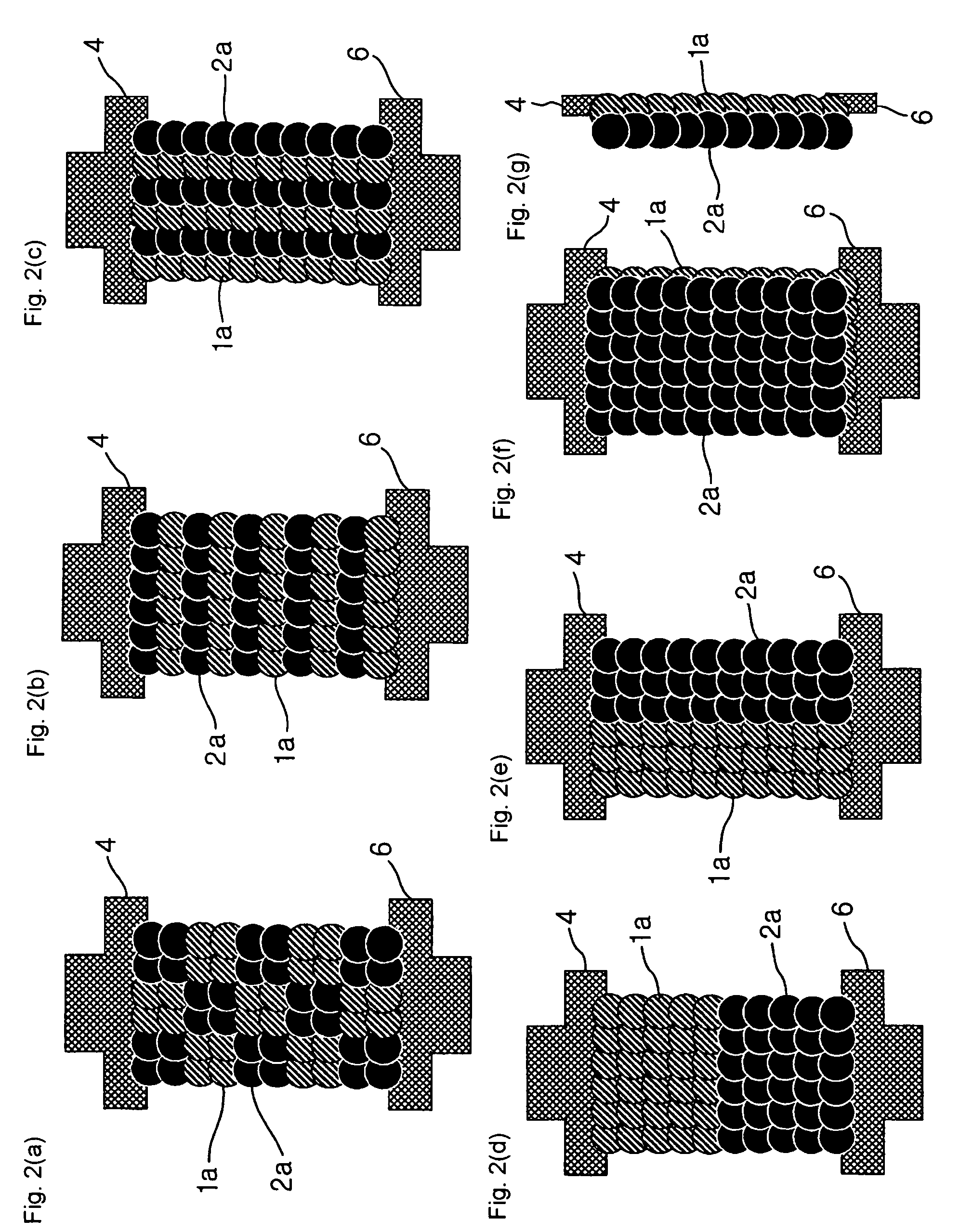
[0104]The pattern shown in the plan view of FIG. 6(a) includes first groups disposed at the terminal 4 side and second groups disposed at the terminal 6 side, like the pattern shown in FIG. 2(d). The first group 1s is defined by a plurality of (4 by 6 in the figure) dots 1a of resistive ink 1 arranged in a rectangular manner, and the second group 2s is defined by a plurality of (4 by 6 in the figure) dots 2a of resistive ink 2 arranged in a rectangular manner. Third groups and fourth groups are disposed in a staggered manner like the pattern shown in FIG. 2(a) in a region 5s between the first group 1s and the second group 2s. Each third group is defined by a plurality of dots 1a of resistive ink 1 as in the pattern shown in FIG. 2(a), and each fourth group is defined by a plurality of dots 2a of resistive ink 2. The dots 1a and 2a overlap each other and thus the first to the fourth group are continuous.

[0105]The patte...


PUM

PropertyMeasurementUnit
temperatureaaaaaaaaaa
viscosityaaaaaaaaaa
viscosityaaaaaaaaaa

Abstract

To provide an electronic component including a resistor element that can be efficiently produced with a range of resistances, and a method for manufacturing the electronic component, the electronic component includes a pair of terminals, and a resistor element disposed between the terminals. The resistor element includes at least two resistive portions (hereinafter referred to as a first resistive portion and a second resistive portion) that are continuously disposed. The first resistive portion includes a plurality of first dots overlapping one another. The second resistive portion includes a plurality of second dots having a different electric resistance from that of the first dots overlapping one another.

Description

CROSS-REFERENCE TO RELATED APPLICATIONS[0001]This is a continuation under 35 U.S.C. § 111 (a) of PCT / JP2007 / 051735 filed Feb. 1, 2007, and claims priority of JP2006-027594 filed Feb. 3, 2006, both incorporated by reference.BACKGROUND[0002]1. Technical Field[0003]The present disclosure relates to electronic components and methods for manufacturing the same. More specifically, the invention relates to an electronic component having a resistor element and a method for manufacturing the same.[0004]2. Background Art[0005]Screen printing, an ink jet method, and other methods are known as techniques for forming a resistor element, such as a resistive film having a desired resistance, for a resistor or the like.[0006]For example, Patent Document 1 discloses that a substantially band-like first resistive portion defined by dots having different areas disposed at different intervals and a second resistive portion having a different electric resistance from the first resistive portion are cont...

Claims


Application Information

Patent Timeline
Patent Type & Authority Patents(United States)
IPC IPC(8): H01C1/012
CPCH01C7/003H01C17/06506Y10T29/49099
Inventor GOTO, SEIJIKIMURA, MASAHIRO
Owner MURATA MFG CO LTD
Why Eureka
Try Eureka