

Layered structure with printed elements
a layered structure and printed element technology, applied in the direction of secondary cells servicing/maintenance, printed circuit non-printed electric components association, instruments, etc., can solve the problems of introducing electronic components prior to incorporating electronic components, presenting significant difficulties, and limited implementation, so as to achieve rapid and efficient structure production, efficient addition to printing line, and convenient use
- Summary
- Abstract
- Description
- Claims
- Application Information
AI Technical Summary
Benefits of technology
Problems solved by technology
Method used
Image

Examples
example 1
Discrete Component Placement and Multilayered Circuit
[0109]Consistent with the teachings above, the invention will now be illustrated in a construction with two composite layers, a base layer 220 and cover layer 210, shown in FIG. 6, which are then laminated together to form the core electronic structure.
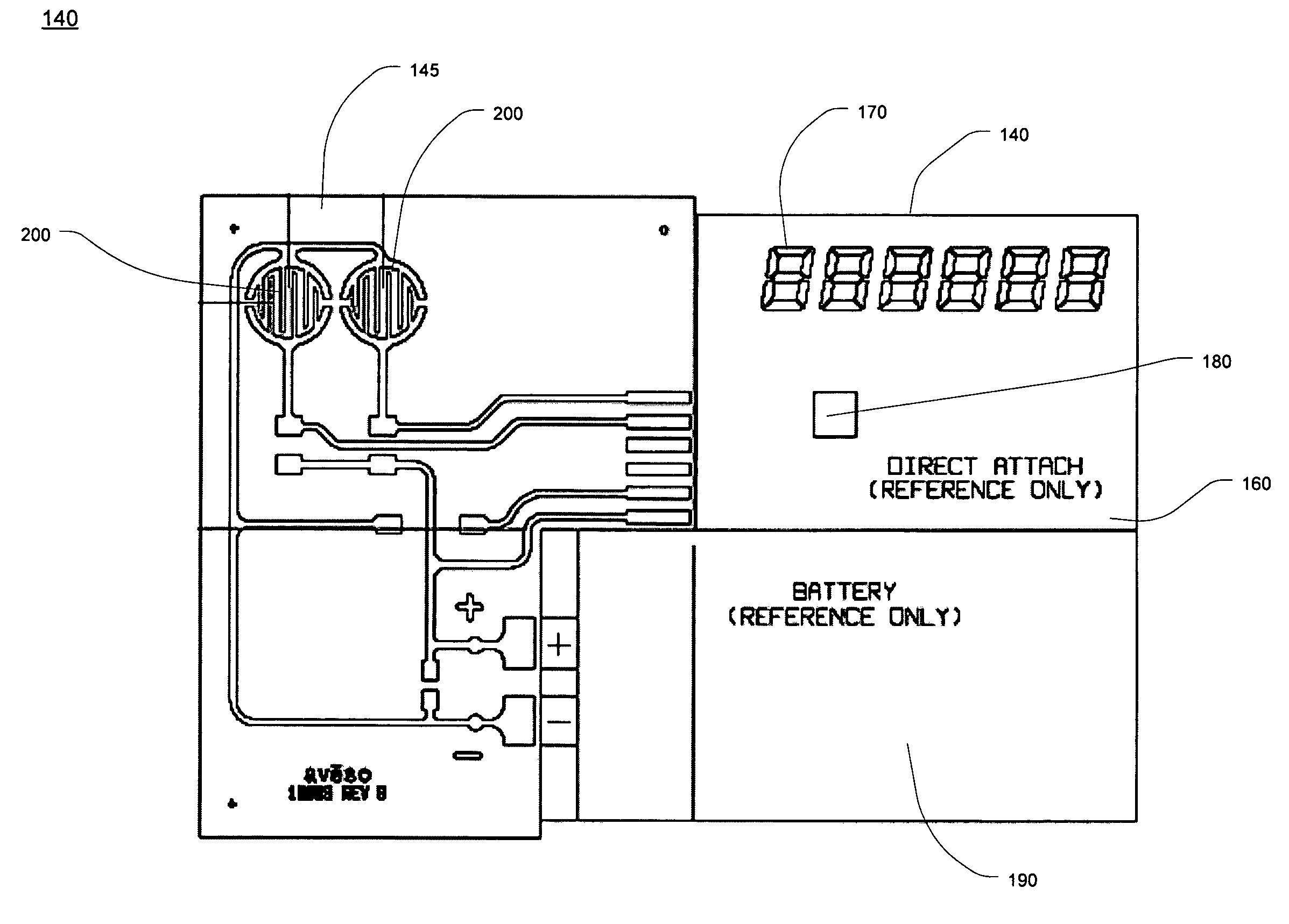
[0110]The electronic core is constructed by placing the necessary components on a base sheet 150 in the proper configuration for the part layout. The base sheet may be PVC or other film which will laminate to outside layers through the hot lamination process. The thickness of the base sheet will preferably be in the range of 0.001 to 0.005 inches with a preferred thickness of 0.002 inches. The various components are held in place with a thin layer of pressure sensitive adhesive.
[0111]The components placed on the base sheet 150 include membrane switch domes, the battery and display cell. The initial component placement determines the spacing of the relief areas as well as the various...
example 2
Planar Circuit and Electrical Connects
[0118]In another example, the construction of base layer 220 is modified by printing the entire connecting circuit on the top of the structure which will match up with the connection points of the display cell and battery components and contain the base for the switches. Electrical connection between the connecting circuit and the components is then provided through needle dispensing to provide a conductive path to each connection. The remaining structure remains the same as Example 1.
[0119]Examples 1 and 2 illustrate the inherent flexibility of printing circuitry within the electronic core. The electronic core will typically have 5-7 discrete surfaces to print circuit elements prior to final assembly. This embodiment of the invention provides the capability to layer the circuitry within the core and use all available surfaces to fit the necessary circuits. This is useful when elaborate circuits must be contained within the area available for a ...
example 3
Embedded Carbon / Zinc Battery
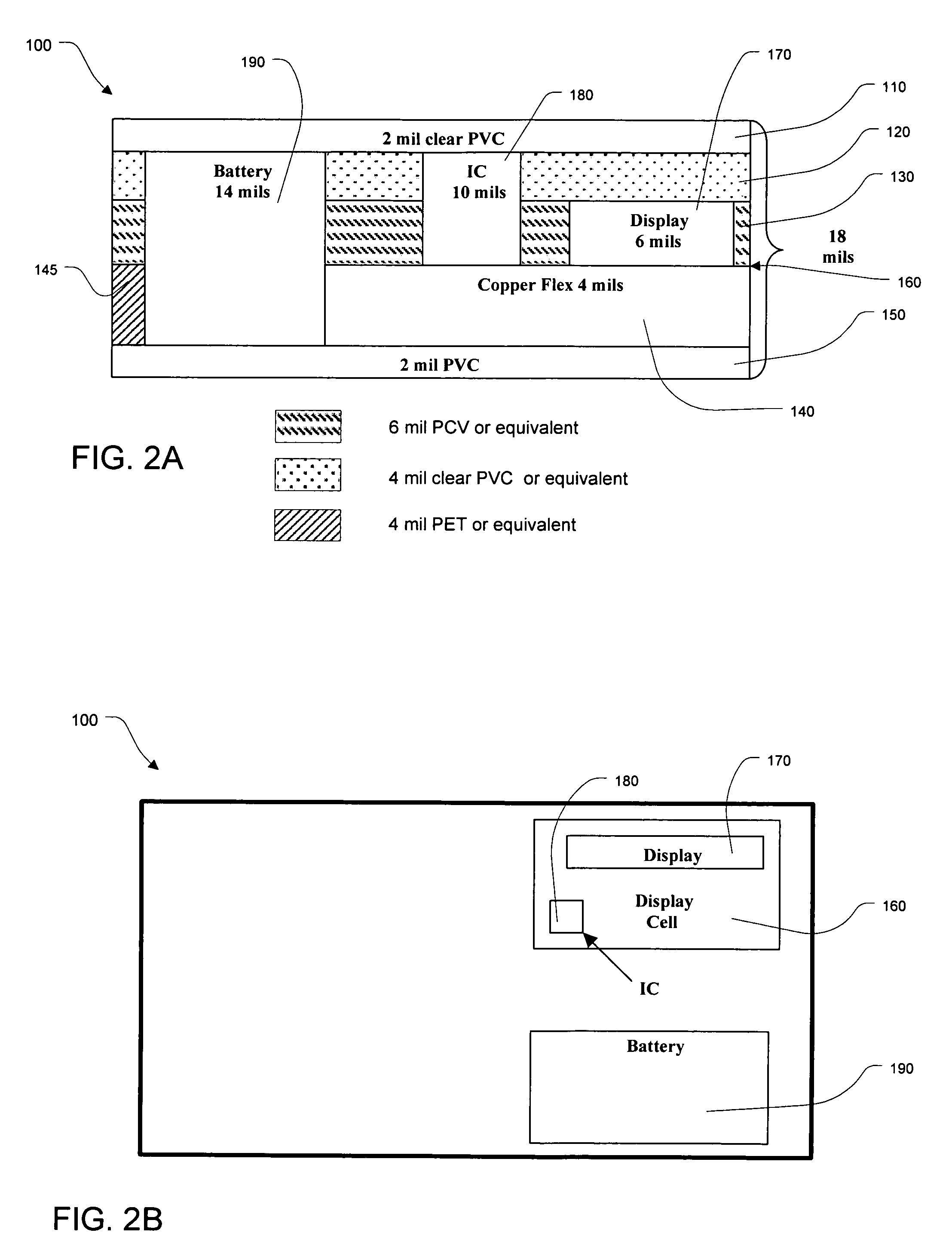
[0121]As described, batteries suitable for use in a smart card are typically 0.012 to 0.016 inches in total thickness. Of that total thickness, 0.006 to 0.010 inches are comprised of packaging films to seal the battery. This example illustrates the use of core layers as part of the battery packaging which saves overall thickness and complexity of the core.
[0122]This construction is based on the base layer 220 / cover layer 210 as described in Example 1. On the base layer, the battery anodes and current collectors are deposited on the top of the second film PVC layer 150. Separately, on the same layer, the cathodes and current collectors are printed as well. The total thickness of the battery layers is 0.006 inches which matches the height of the display. Two separate cells are required to achieve the required 3V from the system. The attach circuitry connects the batteries in series to the other elements.
[0123]The cover layer 210 is constructed to have a eva...
PUM
| Property | Measurement | Unit |
|---|---|---|
| melt temperature | aaaaa | aaaaa |
| thickness | aaaaa | aaaaa |
| heights | aaaaa | aaaaa |
Abstract
Description
Claims
Application Information