Liquid crystal panel having dual column spacer and manufacturing method thereof

a liquid crystal panel and spacer technology, applied in non-linear optics, instruments, optics, etc., can solve the problems of difficult to use the photo acryl layer, narrow viewing angle, disadvantageous tn mode lcd, etc., to improve the resistance to gravity failure, improve the aperture ratio, and improve the resistance to pressing (or painting) failure of the liquid crystal panel

Active Publication Date: 2009-10-27
LG DISPLAY CO LTD
View PDF6 Cites 14 Cited by
  • Summary
  • Abstract
  • Description
  • Claims
  • Application Information

AI Technical Summary

Benefits of technology

[0029]An advantage of the present invention is to provide a liquid crystal panel and a method of manufacture thereof, wherein the aperture ratio can be improved, and resistance to gravity failure, touch spots, pressing (or painting) failure of the liquid crystal panel can be improved by including advantages of the photo acryl pixel structure and the dual column spacer structure.

Problems solved by technology

The TN mode LCD is disadvantageous in that it has a narrow viewing angle.
However, it is difficult to use the photo acryl layer 44′ with the dual column space structure of the related art.

Method used


Image

  • Liquid crystal panel having dual column spacer and manufacturing method thereof
  • Liquid crystal panel having dual column spacer and manufacturing method thereof
  • Liquid crystal panel having dual column spacer and manufacturing method thereof

Examples


first embodiment

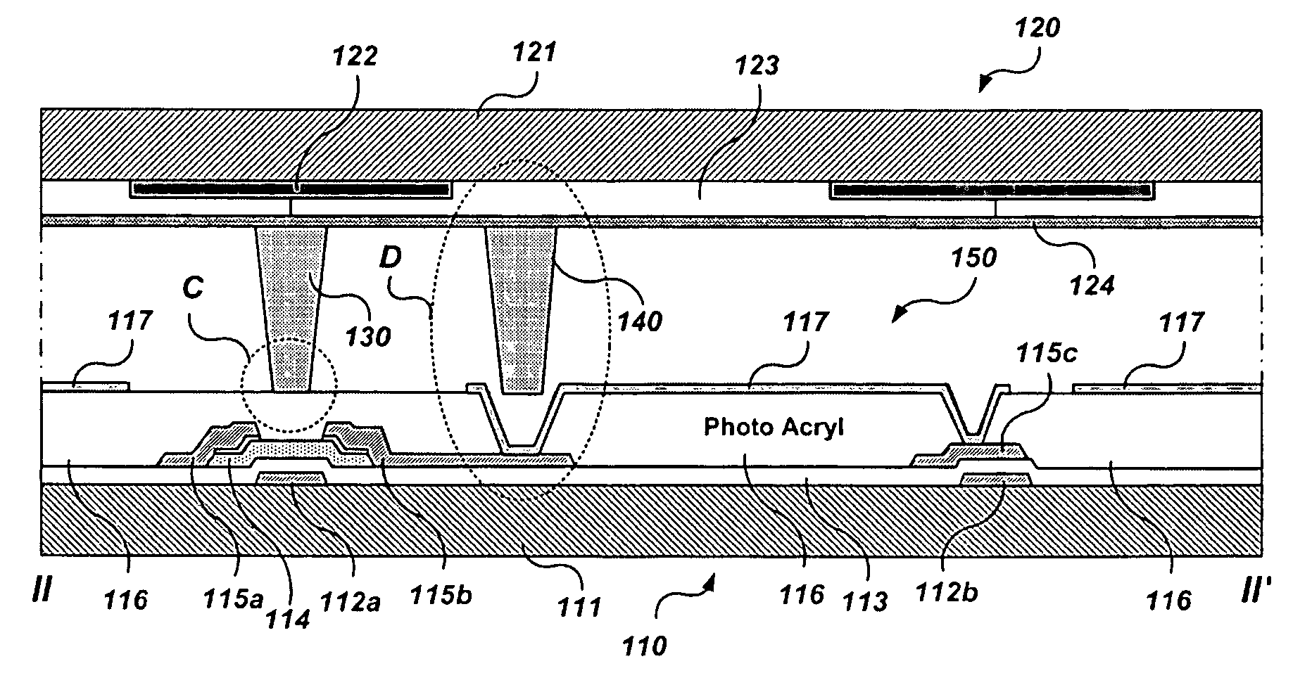
[0052]FIG. 3 is a schematic layout diagram showing the construction of a liquid crystal panel according to the present invention.

[0053]Referring to FIG. 3, the liquid crystal panel having a dual column spacer according to the first embodiment of the present invention includes a first column spacer 130 and a second column spacer 140. The first column spacer 130 is formed over a TFT formation region corresponding to a black matrix region of a color filter substrate. The second column spacer 140 is formed over a drain electrode 115b of a pixel region corresponding to a color filter region of the color filter substrate. The first column spacer 130 serves as a gap spacer for maintaining the gap between a TFT array substrate and the color filter substrate. The second column spacer 140 serves as a pressing spacer and is separated from the TFT array substrate by a predetermined distance.

[0054]The TFT is formed at the crossing of a gate line 112a and a data line 115a. The first column spacer...

second embodiment

[0083]FIG. 7 is a schematic layout diagram of a liquid crystal panel according to the present invention.

[0084]Referring to FIG. 7, the liquid crystal panel having a dual column spacer according to the second embodiment of the present invention includes a first column spacer 130 and a second column spacer 140′. The first column spacer 130 is formed on a TFT formation region corresponding to a black matrix region of a color filter substrate. The second column spacer 140′ is formed over a charge capacitor of a pixel region corresponding to a color filter region of the color filter substrate. The first column spacer 130 serves as a gap spacer for maintaining the gap between a TFT array substrate and the color filter substrate. The second column spacer 140′ serves as a pressing spacer that is spaced apart from the TFT array substrate at a predetermined distance.

[0085]Furthermore, a TFT is formed at the crossing of a gate line 112a and a data line 115a. The first column spacer 130 is form...


PUM

PropertyMeasurementUnit
thicknessaaaaaaaaaa
thicknessaaaaaaaaaa
areaaaaaaaaaaa

Abstract

Disclosed is a liquid crystal panel having a dual column spacer and a manufacturing method thereof. The liquid crystal panel includes a first substrate on which a polished organic insulation film is formed on the entire surface of a pixel region including a TFT. The first substrate includes a contact hole formed through the organic insulation film; a second substrate disposed opposite to the first substrate and having a black matrix and a color filter; a first column spacer formed on the second substrate to contact the first substrate to maintain a gap between the first substrate and the second substrate; and a second column spacer formed on the second substrate on an area of the second substrate corresponding to the contact hole on the first substrate. The second column spacer is separated from the first substrate by a predetermined distance.

Description

[0001]This application claims the benefit of Korean Patent Application No. 2005-0058863, filed on Jun. 30, 2005, which is hereby incorporated by reference for all purposes as if fully set forth herein.BACKGROUND OF THE INVENTION[0002]1. Field of the Invention[0003]The present invention generally relates to a liquid crystal display device, and mote particularly, to a liquid crystal panel having a dual column spacer structure and a manufacturing method thereof.[0004]2. Discussion of Related Art[0005]A liquid crystal display device displays images by employing the optical anisotropy and birefringence properties of liquid crystal molecules. A typical liquid crystal display device includes two opposing substrates each having electric field generating electrodes disposed on a surface facing the other substrate. A liquid crystal layer is formed between the two substrates. The orientation of liquid crystal molecules of the liquid crystal is then changed by means of an electric field generat...

Claims


Application Information

Patent Timeline
Patent Type & Authority Patents(United States)
IPC IPC(8): G02F1/1339
CPCG02F1/13394G02F1/133512G02F2201/50G02F1/136227G02F1/1339
Inventor KIM, PYUNG HUN
Owner LG DISPLAY CO LTD
Why Eureka
Try Eureka