Design of CMOS integrated germanium photodiodes

a technology of integrated germanium and photodiodes, which is applied in the direction of optical elements, manufacturing tools, instruments, etc., can solve the problems of less sensitive and/or noisy devices, and achieve the effects of reducing optical scattering losses and/or optical absorption losses, improving integrated waveguide photodiodes, and improving the effect of integrated waveguide photodiodes

Active Publication Date: 2009-11-03
CISCO TECH INC
View PDF3 Cites 35 Cited by
  • Summary
  • Abstract
  • Description
  • Claims
  • Application Information

AI Technical Summary

Benefits of technology

[0011]The current invention is an improved integrated waveguide photodiode. According to the current invention, optical losses associated with contacts to the germanium layer of the silicon and germanium photodiode are reduced by positioning the contacts in proximity to predicted low optical field regions at the top surface of the germanium layer. In some cases, the low optical field regions may be predicted based on modeling and / or experimental data. In some examples according to the current invention, careful contact positioning may result in reduced optical scattering losses and / or optical absorption losses associated with the contacts. Reduced optical losses may result in more sensitive and / or less noisy devices. In some cases, design rules may be altered to incorporate the reduced optical losses and smaller and / or more compact devices may be designed and / or manufactured.
[0012]According to the current invention, lateral confinement of light in the silicon layer of the silicon and germanium photodiode may be improved and optical losses may be reduced by establishing side trenches along at least some portion of the length of the photodiode. In depth, the side trenches extend at least partially into the silicon layer; in length, the side trenches are adjacent to the germanium detector. In some cases, the trenches may be substantially parallel to the edge of the germanium layer in the photodiode. In some cases, the trenches may vary in width. For example, in some examples according to the current invention, trenches may be used in conjunction with a tapered germanium layer. In some cases, the trench edges closest to the tapered germanium layer may be substantially parallel to the edge of the tapered germanium layer, whereas the far edges of the trenches may or may not be parallel to the tapered germanium layer. In some cases, the side trenches are filled with a dielectric material such as, but not limited to, a silicon-oxi-nitride (SiOxNy) dielectric. Reduced optical losses in the silicon layer of the silicon and germanium photodiode portion of the integrated waveguide photodiode may enable more efficient coupling of optical power from the silicon layer to the germanium layer, possibly resulting in more sensitive and / or less noisy devices. In some cases, design rules may be altered to incorporate the reduced optical losses and smaller and / or more compact devices may be designed and / or manufactured.
[0013]According to the current invention, a novel taper structure may be used to reduce optical losses when light is injected from the silicon layer to the germanium layer of a germanium on silicon integrated waveguide photodiode. For some examples of the current invention, the novel taper structure may be used to increase the overlap of the light with the germanium, to reduce the length of the waveguide photodiode while maintaining responsivity, and / or to reduce the detrimental impact of other loss mechanisms. According to the current invention, the geometry of a taper in the germanium layer of the silicon and germanium photodiode is selected at least in part based on the desirability of the expected operational modes for a multimode system. Preferred geometries would support modes which anti-cross, converting unattractive modes into attractive modes. For example, an attractive mode might have a high overlap with the germanium layer, thereby improving the absorption in the germanium layer which may lead to attractive device characteristics. In some cases, different and / or additional considerations may be used to identify attractive modes such as, but not limited to, identifying modes which are “non-leaky” or have good lateral confinement. Modal analysis based on proposed geometries, coupling coefficients from the silicon waveguide into the integrated waveguide photodiode, and / or the effective indices of predicted dominant modes may be used, at least in part, to guide the design of a novel taper. According to the current invention, modal analysis may be used to identify an appropriate initial taper width, an intermediate taper width, a taper grade, a final taper width and / or a taper length. In some cases, other considerations may be used to identify appropriate taper parameters such as, but not limited to, device capacitance considerations and / or manufacturing constraints related to germanium thickness control, minimum feature size and / or manufacturable feature shape.

Problems solved by technology

Reduced optical losses may result in more sensitive and / or less noisy devices.

Method used


Image

  • Design of CMOS integrated germanium photodiodes
  • Design of CMOS integrated germanium photodiodes
  • Design of CMOS integrated germanium photodiodes

Examples


Embodiment Construction

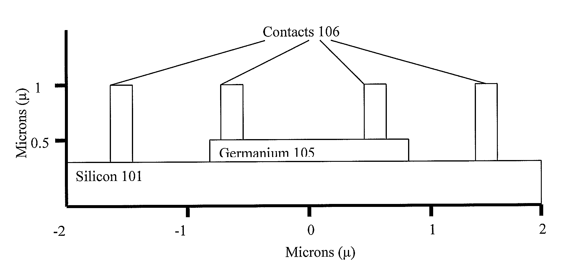
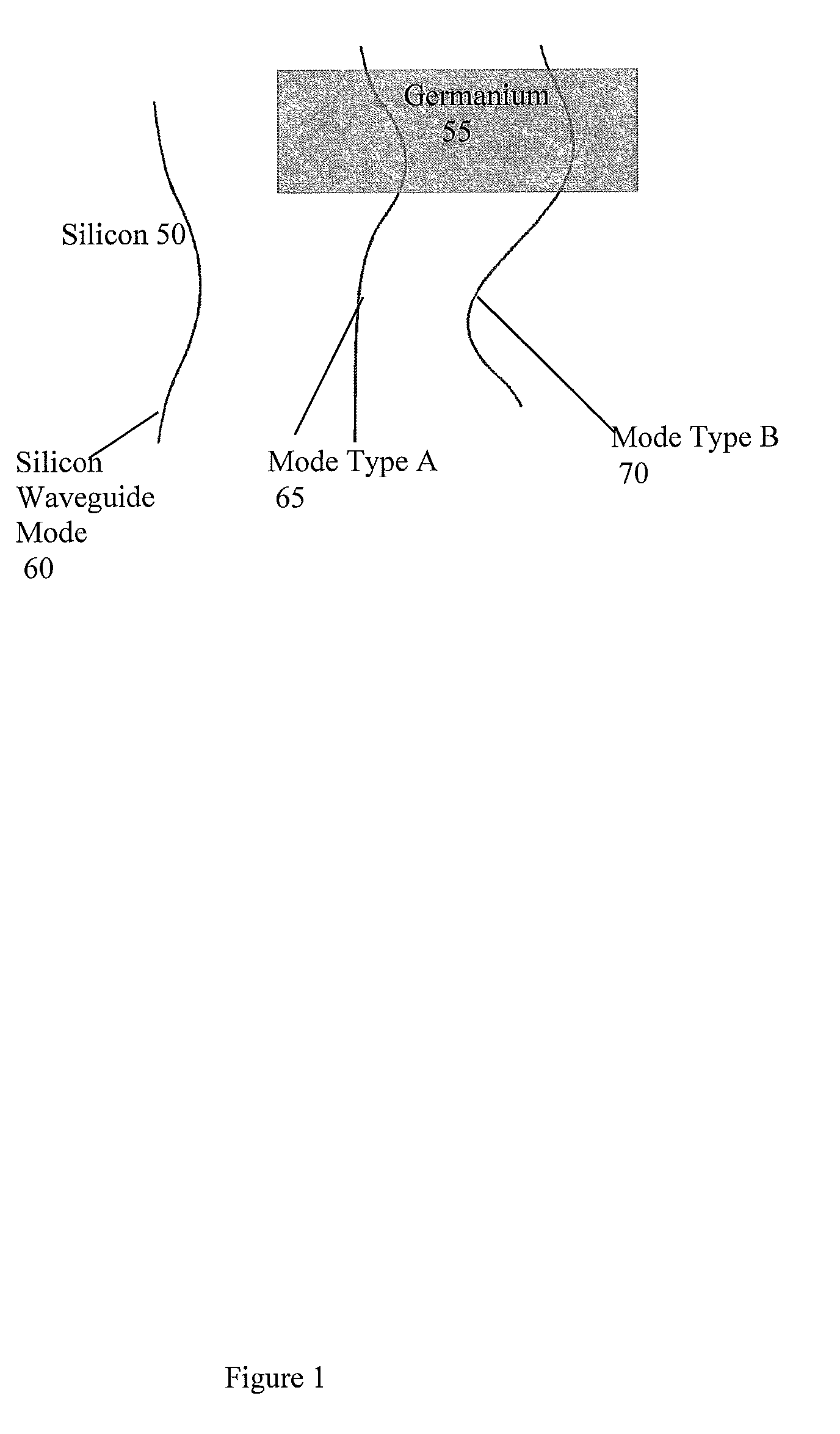
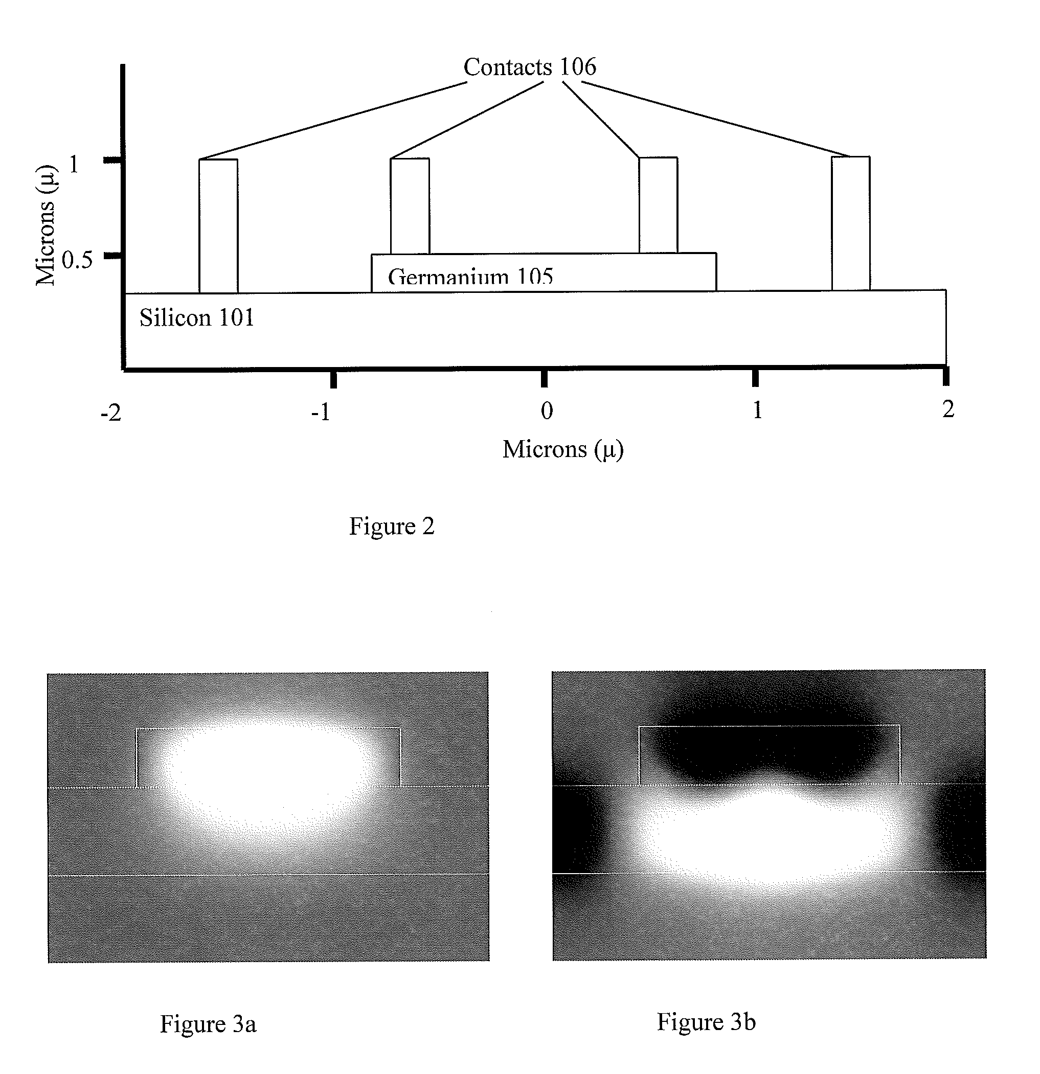
[0048]For the purposes of discussion, modes in photodiodes according to the current invention may be numbered (mode 1 , mode 2 , mode 3) in order according to increasing index and / or typed (type A, type B, type C) according to other properties. Mode 1 (mode type A) is the ground mode of the waveguide photodiodes. It has a single lobe, a high overlap with the germanium, and is well guided by the germanium stripe even in the absence of other structures in the silicon. Mode type B has a vertical lobe structure and a reduced overlap with germanium as compared with mode 1 . Note that vertical refers to the direction normal to the wafer surface. In some cases, it may be only partially guided by the germanium stripe alone; for example, a type B mode may be a leaky mode in the absence of other structures such as, but not limited to, side-trenches. Mode type C has a mode overlap with germanium that is substantially higher than mode type B's overlap with germanium. Mode type C has a mode over...


PUM

PropertyMeasurementUnit
infrared wavelengthaaaaaaaaaa
widthaaaaaaaaaa

Abstract

A CMOS processing compatible germanium on silicon integrated waveguide photodiode. Positioning contacts in predicted low optical field regions, establishing side trenches in the silicon layer along the length of the photodiode reduces optical losses. Novel taper dimensions are selected based on the desirability of expected operational modes, reducing optical losses when light is injected from the silicon layer to the germanium layer. Reduced vertical mismatch systems have improved coupling between waveguide and photodiode. Light is coupled into and / or out of a novel silicon ring resonator and integrated waveguide photodiode system with reduced optical losses by careful design of the geometry of the optical path. An integrated waveguide photodiode with a reflector enables transmitted light to reflect back through the integrated waveguide photodiode, improving sensitivity. Careful selection of the dimensions of a novel integrated waveguide microdisk photodiode system results in reduced scattering. Improved sensitivity integrated waveguide photodiodes comprise integrated heaters.

Description

CROSS-REFERENCE TO RELATED APPLICATIONS[0001]This application is a conversion of and claims priority from U.S. Provisional application No. 60 / 791,867 entitled “Design of CMOS Integrated Germanium Photodiodes”, filed on Apr. 13, 2006, herein incorporated by reference.FIELD OF INVENTION[0002]Invention relates to the design and manufacture of optical devices, specifically to integrated waveguide photodiodes.BACKGROUND OF INVENTION[0003]The rapid expansion in the use of the Internet has resulted in a demand for high speed communications links and devices, including optical links and devices. Optical links using fiber optics have many advantages compared to electrical links: large bandwidth, high noise immunity, reduced power dissipation and minimal crosstalk. Optoelectronic integrated circuits made of silicon are highly desirable since they could be fabricated in the same foundries used to make VLSI integrated circuits. Optical communications technology is typically operating in the 1.3...

Claims


Application Information

Patent Timeline
Patent Type & Authority Patents(United States)
IPC IPC(8): G02B6/12
CPCG02B6/12007
Inventor WITZENS, JEREMYMASINI, GIANLORENZOCAPELLINI, GIOVANNIGUNN, III, LAWRENCE C.
Owner CISCO TECH INC
Why Eureka
Try Eureka