Thin film solar cell

a thin film solar cell and solar cell technology, applied in the field of thin film solar cells, can solve the problems of low efficiency, energy band gap, thin film solar cell, etc., and achieve the effects of reducing work function, improving solar cell efficiency, and increasing energy outpu

Inactive Publication Date: 2014-08-26
BOREALIS TECH LTD
View PDF150 Cites 13 Cited by
  • Summary
  • Abstract
  • Description
  • Claims
  • Application Information

AI Technical Summary

Benefits of technology

[0032]An advantage of the present invention is that since the modified structure of the metal reduces its work function, electrons are emitted from the metal surface at lower energies and can readily combine with holes, created by solar photons, to produce electricity. This improves the efficiency of the solar cell since a greater energy output is produced by a lower energy input.
[0033]A further advantage of the present invention is that the natural resistance present between the metal back contact and the semiconductor layer above it is reduced. Current losses at the back contact are therefore minimised, increasing the output current of the device.
[0034]Yet a further advantage of the present invention is the reduction in collection losses, which are caused by delayed recombination of electrons and holes between the p-n junction of the solar cell and the metal back contact. The reduced work function of the metal allows electrons and holes to combine more quickly and at lower energies, leading the generation of useful electricity rather than wasted heat.
[0035]A further advantage of the present invention is that it can be readily manufactured using inexpensive materials.
[0036]In a further embodiment of the present invention the semiconductor absorber layer, disposed on the surface of the metal back contact, is also modified with nanoscale indentations or protrusions. These have the effect of changing the size of the band gap in the semiconductor and thus altering the absorption properties of the solar cell.
[0037]An advantage of this embodiment of the present invention is that, due to the modification of the semiconductor absorber layer, the size of the band gap in the semiconductor is tuned. An optimum band gap, facilitating maximum possible solar-electric energy conversion, can thus be selected and the sensitivity of the solar cell extended to include lower energy photons.

Problems solved by technology

In the case that the potential barrier does not allow tunneling, providing indents on a surface of a metal creates for that metal an energy band gap due to de Broglie wave interference inside the metal.
The typical thin film solar cell described has several disadvantages, the major one being its low efficiency.
The efficiency of the solar cell is thus severely limited.
Attempts at controlling the band gap of the absorber by the introduction of quantum dots are currently challenged by inefficient charge carrier transport mechanisms outside the quantum dots.
Potential power is also lost when electrons and holes combine between the p-n junction and back contact, thereby generating heat rather than electricity.
This mechanism is the cause of collection losses and further reduces the efficiency of thin film solar cells.
This resistance tends to impede current flow through the external circuit, thus further diminishing the power output of the device.
Due to the low power output, operating a solar cell is relatively expensive.
This makes the solar cell a poor competitor in the energy generation market.

Method used


Image

  • Thin film solar cell
  • Thin film solar cell
  • Thin film solar cell

Examples


Embodiment Construction

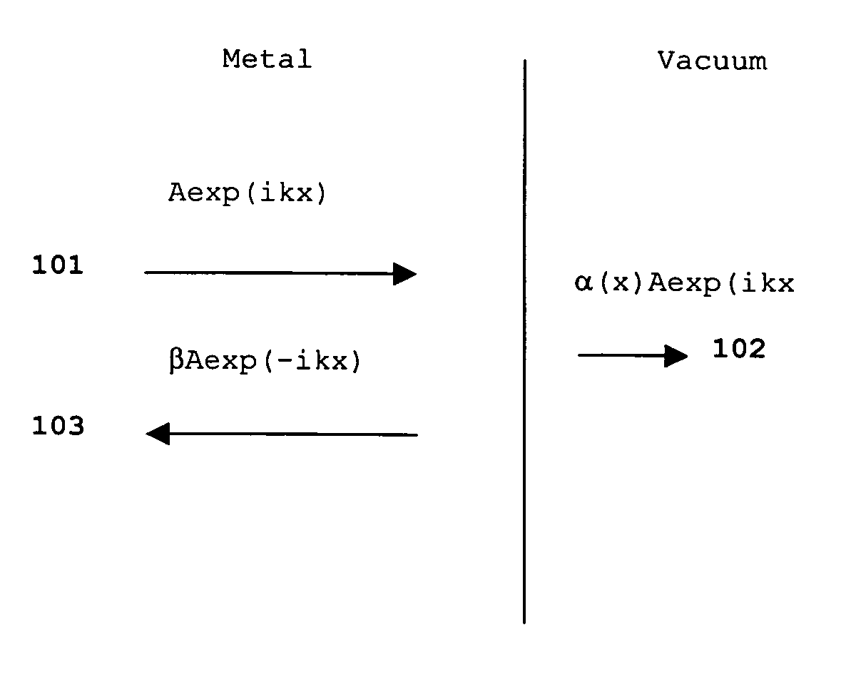
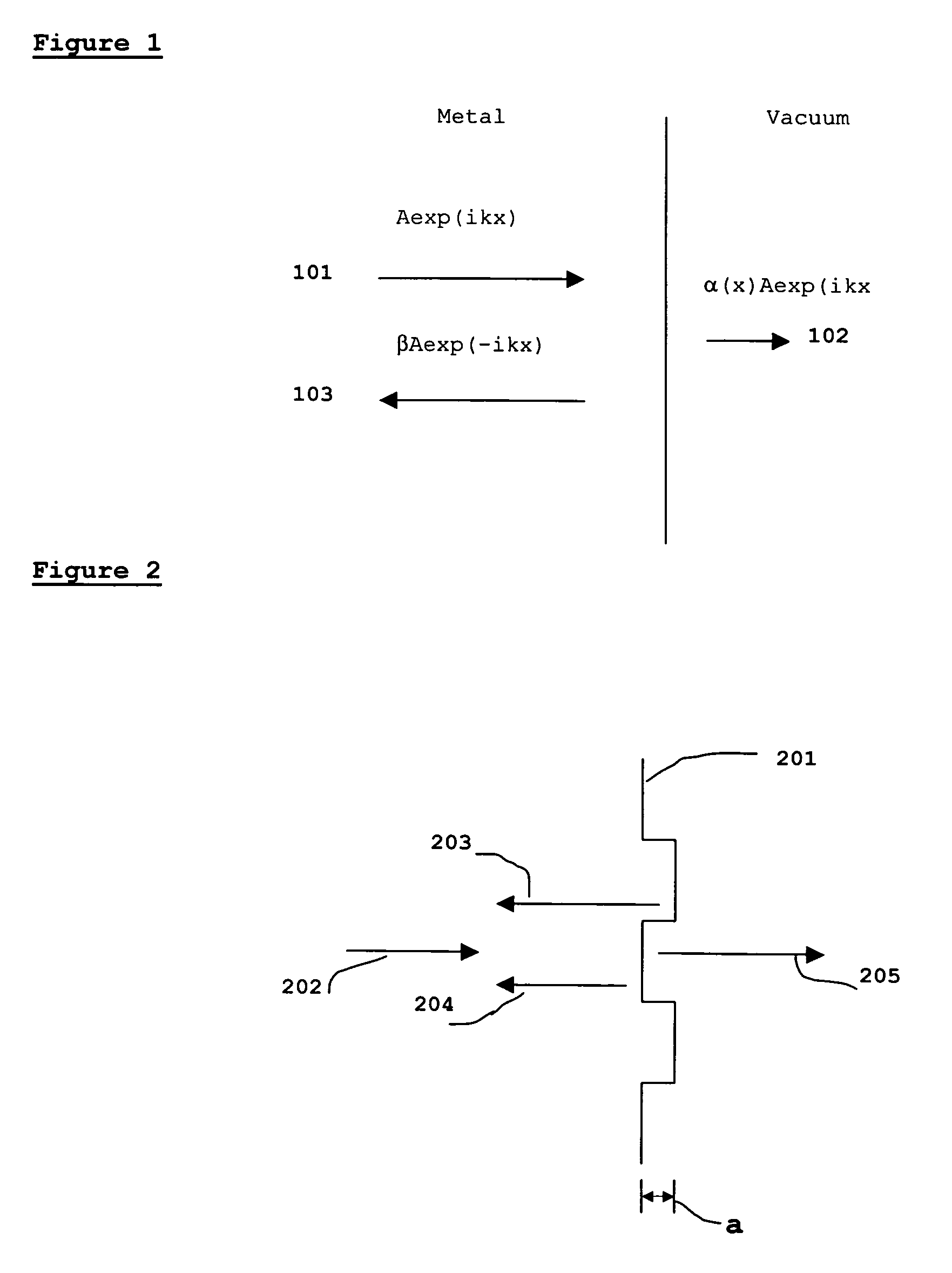
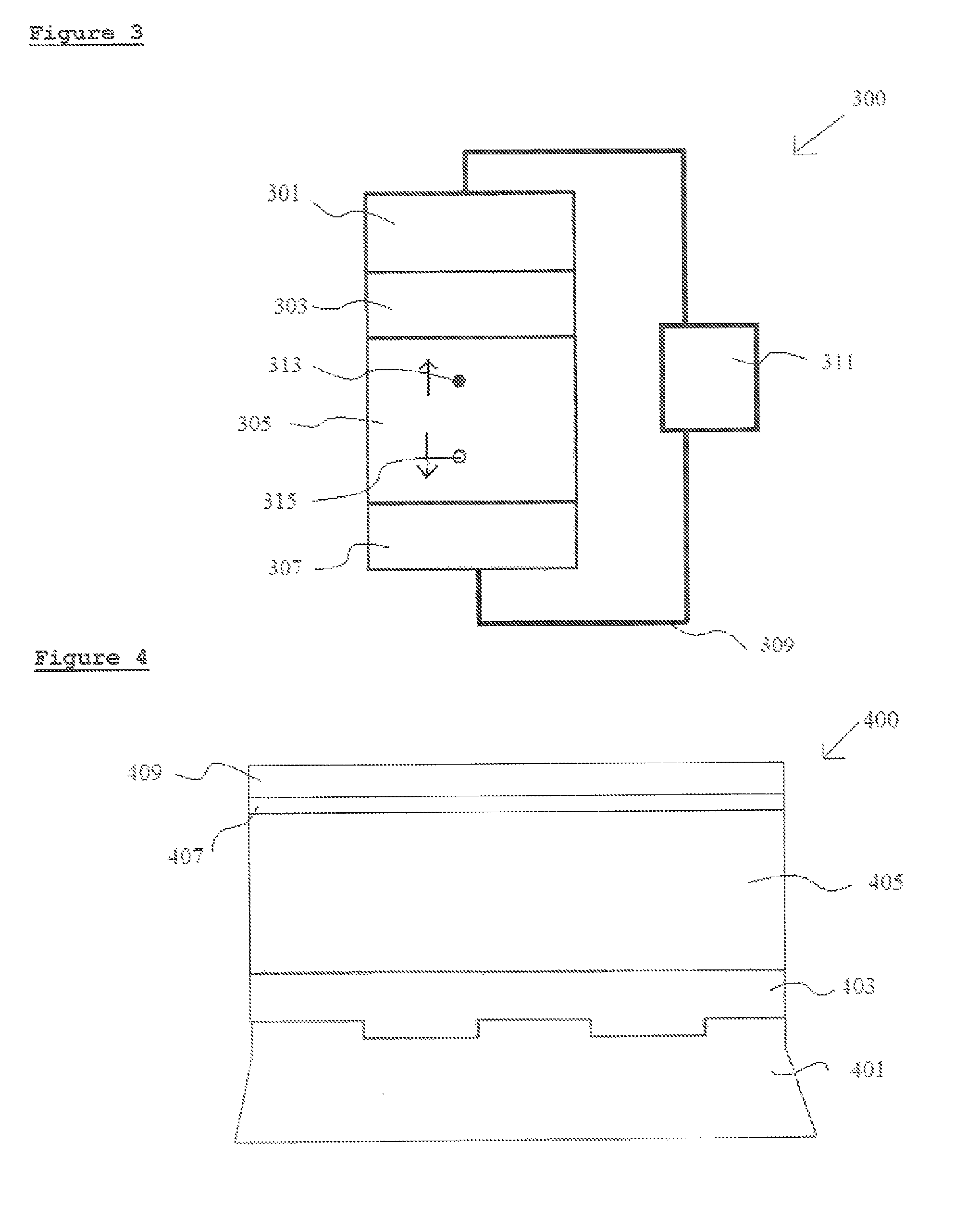
[0049]The embodiments of the present invention and its technical advantages are best understood by referring to FIGS. 4-5. The present invention relates to a thin film solar cell, in which the structure of the metal back contact is modified, thereby improving the efficiency of the cell.

[0050]Referring now to FIG. 4, which shows a cross sectional view of the thin film solar cell of the present invention. Shown is solar cell 400 comprising carrier layer, 401, metal back contact, 403, p-type semiconductor absorber layer, 405, n-type semiconductor collector layer 407 and ZnO window layer 409.

[0051]The surface of carrier layer 401 is modified with nanoscale indentations or protrusions to have a periodically repeating structure of one or more indents or protrusions. Methods for carrying this out are well known to those skilled in the art and include screen printing, as used for printing CD surfaces, electron beam lithography and other imprinting processes. In a preferred embodiment of the...


PUM

PropertyMeasurementUnit
widthaaaaaaaaaa
depthaaaaaaaaaa
thicknessaaaaaaaaaa

Abstract

An improved efficiency thin film solar cell is disclosed. Nanoscale indentations or protrusions are formed on the cross sectional surface of a carrier layer, onto which a thin metal film is deposited. Additional layers, including semiconductor absorber and collector layers and a window layer, are disposed on the metal film, thereby completing the solar cell. The nanostructure underlying the metal film serves to reduce the work function of the metal and thereby assists in the absorption of holes created by solar photons. This leads to more efficient electricity generation in the solar cell. In a further embodiment of the present invention the cross sectional surface of the semiconductor absorber layer is also modified by nanoscale indentations or protrusions. These indentations or protrusions have the effect of altering the size of the semiconductor band gap, thereby optimizing the radiation absorption properties of the solar cell.

Description

CROSS-REFERENCE TO RELATED APPLICATIONS[0001]This application claims the benefit of U.S. Provisional Patent Application No. 60 / 900,602, filed Feb. 9, 2007.BACKGROUND OF THE INVENTION[0002]The present invention relates to thin film solar cells.[0003]A) Increasing Emission Through a Potential Barrier by Altering the Surface Structure of the Potential Barrier.[0004]In U.S. Pat. No. 6,680,214 and U.S. Pat. App. No. 2004 / 0206881 methods are disclosed for the induction of a suitable band gap and electron emissive properties into a substance, in which the substrate is provided with a surface structure corresponding to the interference of electron waves.[0005]The space distribution of the probability wave associated with an elementary particle is given by:ψ*=Aexp(ikr)  (1)[0006]where k is the wave number and r is a vector connecting initial and final locations of the particle.[0007]FIG. 1 shows incident wave 101 Aexp(ikx) moving from left to right perpendicular to a surface dividing two dom...

Claims


Application Information

Patent Timeline
Patent Type & Authority Patents(United States)
IPC IPC(8): H01L31/00
CPCH01L31/00H01L31/0749H01L31/02366H01L31/03928Y02E10/541Y02P70/50
Inventor WALITZKI, HANS, JUERGEN
Owner BOREALIS TECH LTD
Why Eureka
Try Eureka