Method of making a transistor with a sloped drain diffusion layer

a diffusion layer and transistor technology, applied in the field of manufacturing methods of semiconductor devices, can solve the problems of increasing the manufacturing process to require a high manufacturing cost, increasing the manufacturing cost, and complicated manufacturing process, so as to suppress the manufacturing cost, reduce the number of masks, and reduce the effect of mask siz

Inactive Publication Date: 2009-12-08
SEMICON COMPONENTS IND LLC
View PDF15 Cites 4 Cited by
  • Summary
  • Abstract
  • Description
  • Claims
  • Application Information

AI Technical Summary

Benefits of technology

[0011]In view of the aforementioned circumstances, a method of manufacturing a semiconductor device of the present invention includes the steps of forming a backgate diffusion layer on a semiconductor layer and then forming a gate oxide film and a gate electrode on the semiconductor layer, and implanting impurity ions into the backgate diffusion layer and thereafter diffusing the impurity ions thereinto to form a source diffusion layer and a drain diffusion layer, in which in the step of forming the drain diffusion layer, the drain diffusion layer is formed in order that the drain diffusion layer has a slope relative to a surface of the semiconductor layer and an angle formed by a tangent line of the slope and the surface of the semiconductor layer gets smaller toward the surface of the semiconductor layer. Accordingly, in the present invention, the drain diffusion layer is widely diffused as it approaches to the surface of the semiconductor layer. Then, in the drain diffusion layer, an impurity concentration in the vicinity of the surface of the semiconductor surface becomes low. This manufacturing method makes it possible to realize an electric field relaxation in the drain diffusion layer while reducing the number of masks and that of manufacturing processes to suppress the manufacturing cost.
[0012]Moreover, according to the method of manufacturing a semiconductor device of the present invention, in the step of forming the backgate diffusion layer, a first diffusion layer having a peak of an impurity concentration located at a deeper portion of the semiconductor layer is formed, and thereafter a second diffusion layer having a peak of an impurity concentration closer to the surface of the semiconductor layer than the peak of the impurity concentration of the first diffusion layer, is formed in a way that the first and second diffusion layers are overlapped. Accordingly, in the present invention, the second diffusion layer is formed on the first diffusion layer to form the backgate diffusion layer. This manufacturing method can form the backgate diffusion layer that can realize a concentration profile in which the impurity concentration reaches the peak at the deeper portion and gradually decreases as it approaches to the surface of the semiconductor layer.
[0013]Furthermore, according to the method of manufacturing a semiconductor device, in the step of forming the drain diffusion layer, after the second diffusion layer is formed, the drain diffusion layer is formed by use of the gate electrode as a mask. Accordingly, in the present invention, a low concentration region of the drain diffusion layer can be formed with a high accuracy of position to the gate electrode. This manufacturing method can realize an electric field relaxation in the drain region.
[0014]Still furthermore, according to the method of manufacturing a semiconductor device of the present invention, the gate oxide film is formed to have a thickness of 50 to 340 Å. Accordingly, in the present invention, the thickness of the gate oxide film is reduced, thereby enabling an operation to be performed at a low driving voltage.

Problems solved by technology

This causes a problem in which the number of masks and that of manufacturing processes are increased to require a high manufacturing cost.
Moreover, there is a problem in which the manufacturing process becomes complicated.
However, this manufacturing method causes a problem in which the number of manufacturing processes is increased, resulting in an increase in manufacturing cost.
Moreover, there is a problem in which the manufacturing process becomes complicated.
However, in this manufacturing method, the impurity concentration of the region where the drain region is formed is relatively high, so that the drain region is less likely to be widely diffused in the channel direction and the depth direction.
Then, there is a problem in which a withstand voltage characteristic deteriorates when the semiconductor device is turned on.

Method used


Image

  • Method of making a transistor with a sloped drain diffusion layer
  • Method of making a transistor with a sloped drain diffusion layer
  • Method of making a transistor with a sloped drain diffusion layer

Examples


Embodiment Construction

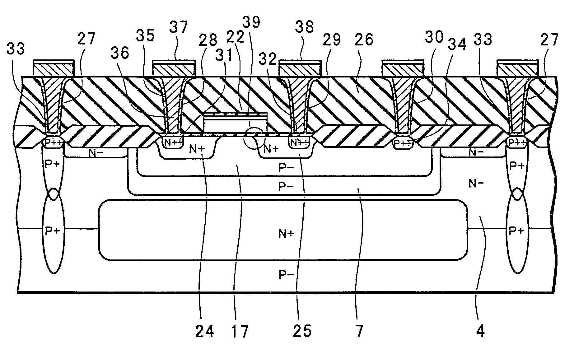
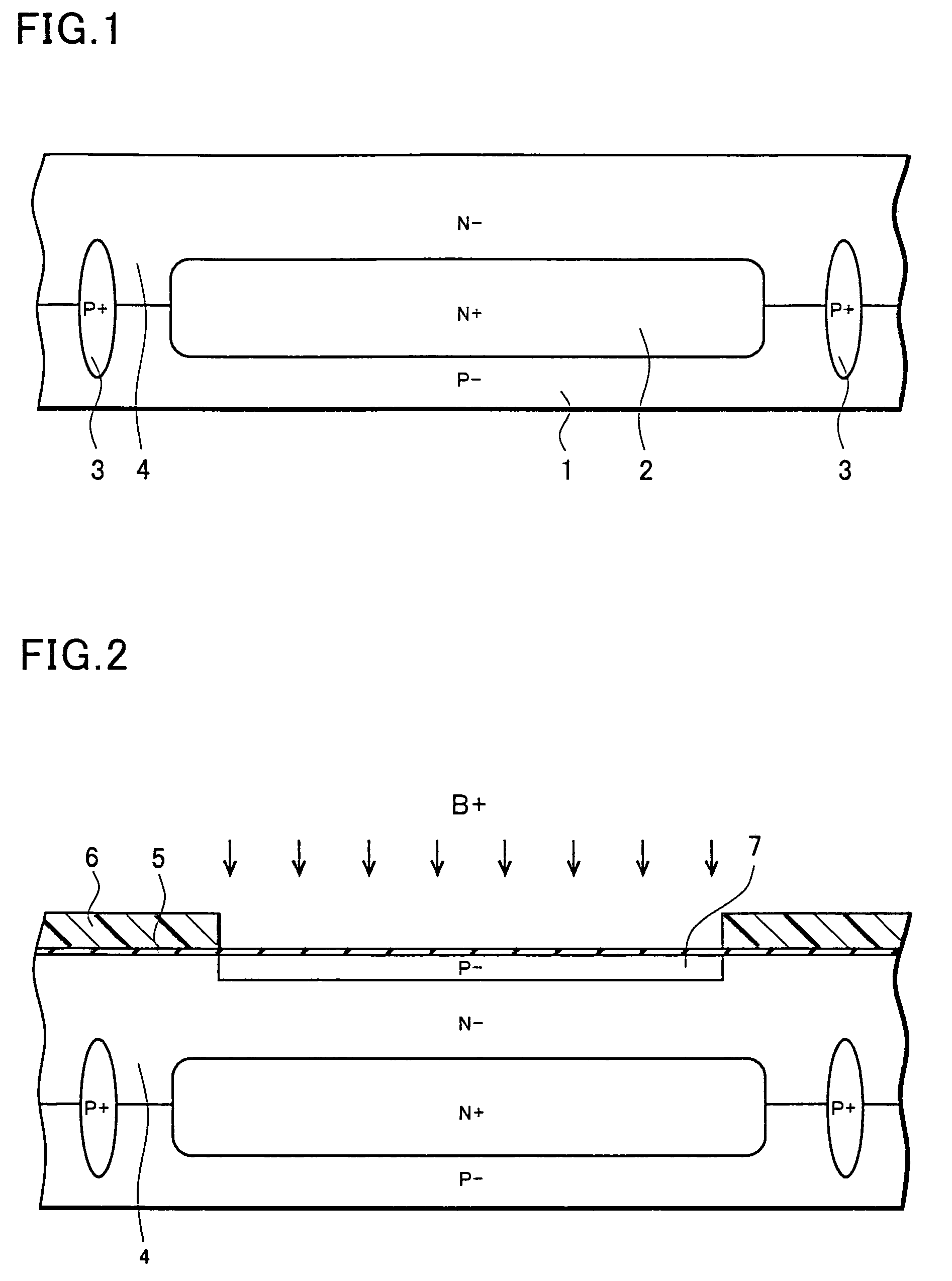
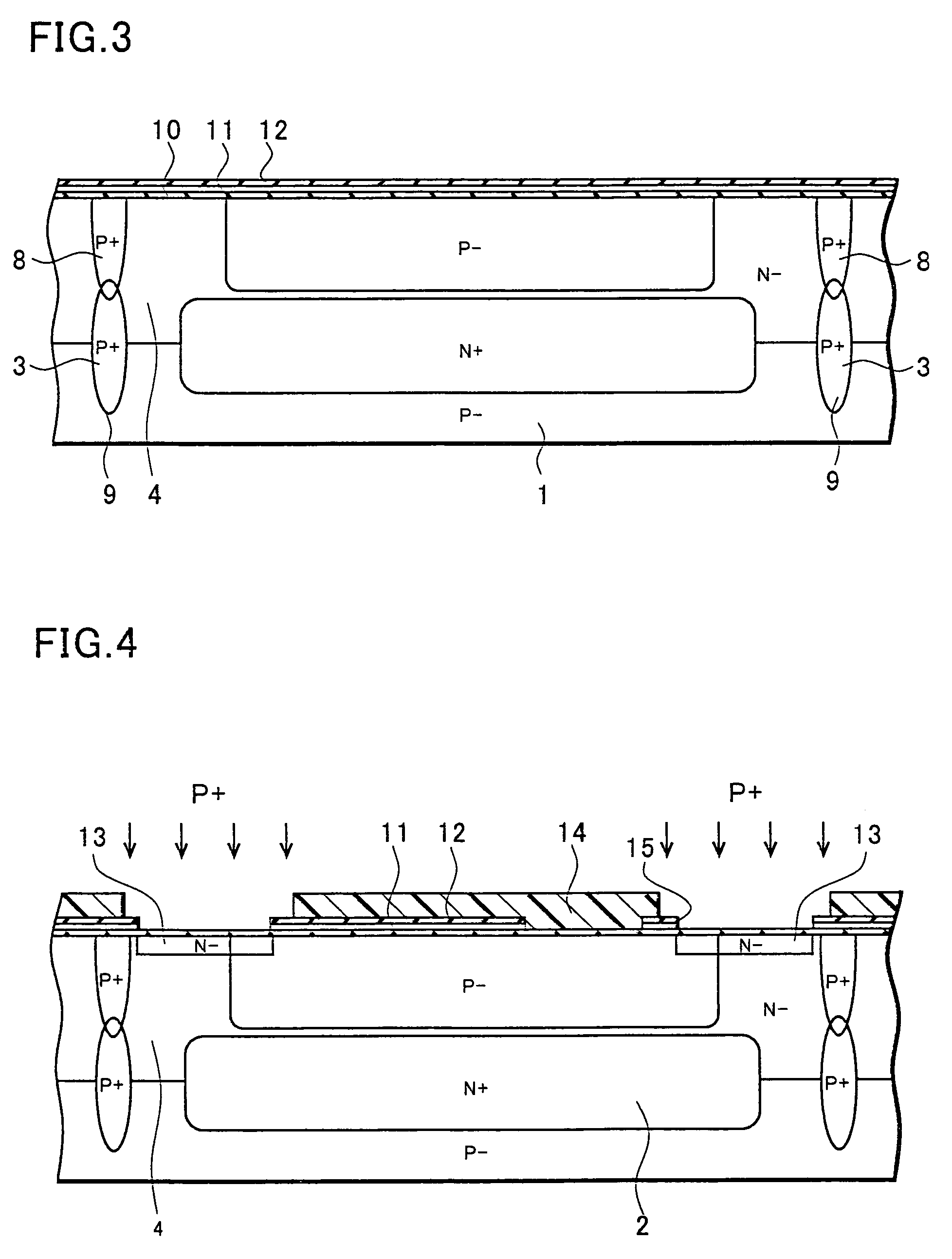
[0028]The following will specifically explain a method of manufacturing a semiconductor device of an embodiment of the present invention with reference to FIGS. 1 to 8. FIGS. 1 to 8 are cross sectional views each explaining the method of manufacturing a semiconductor device according to the embodiment of the present invention. Although the following explains a case in which, for example, an N-channel type MOS transistor is formed in one device forming region divided by an isolation region, the embodiment of the present invention is not limited to this case. For example, the embodiment of the present invention may be applied to a case in which a P-channel type MOS transistor, an NPN type transistor and a vertical PNP transistor are formed in the other device forming region to form a semiconductor integrated circuit device.

[0029]First of all, as illustrated in FIG. 1, a P type monocrystalline silicon substrate 1 is prepared. An N type impurity, for example, phosphorus (P) ions are imp...


PUM


Abstract

Disclosed is that in a method of manufacturing a semiconductor device of the present invention, when first and second P type diffusion layers using as a backgate region, these layers are formed in such a way that their impurity concentration peaks are shifted, respectively. Then, in the backgate region, a concentration profile of a region where an N type diffusion layer is formed is gradually established. After that, impurity ions, which form the N type diffusion layer, are implanted, and thereafter a thermal treatment is performed to diffuse the N type diffusion layer in a y shape at a lower portion of a gate electrode. This manufacturing method makes it possible to implement an electric filed relaxation in a drain region.

Description

[0001]Priority is claimed to Japanese Patent Application Number JP2005-098968 filed on Mar. 30, 2005, the disclosure of which is incorporated herein by reference in its entirety.BACKGROUND OF THE INVENTION[0002]1. Field of the Invention[0003]The present invention relates to a manufacturing method of a semiconductor device for reducing a film thickness of a gate oxide film to relax an electric field in a drain region.[0004]2. Description of the Related Art[0005]In conventional methods of manufacturing a semiconductor device, for example, the following technique is known. A gate oxide film is formed on a P type silicon substrate. A gate electrode formed of polysilicon is formed on the gate oxide film. Then, arsenic ions are implanted into the substrate using the gate electrode by a self-alignment technique to form a low concentration diffusion layer with an LDD (Lightly Doped Drain) structure. Thereafter, a side wall spacer is formed on a side surface of the gate electrode to form a h...

Claims


Application Information

Patent Timeline
Patent Type & Authority Patents(United States)
IPC IPC(8): H01L21/8244
CPCH01L29/0847H01L29/7833H01L29/6659H01L29/1083H01L21/823892H01L29/456H04B10/60
Inventor OTAKE, SEIJIKIKUCHI, SHUICHI
Owner SEMICON COMPONENTS IND LLC
Why Eureka
Try Eureka