Electrical test probe

a technology of electric test and probe, applied in the field of probes, can solve the problems of overdriving to act on each probe, no accurate test can be performed, etc., and achieve the effect of reducing signal disorder

Active Publication Date: 2009-12-08
NIHON MICRONICS
View PDF14 Cites 16 Cited by
  • Summary
  • Abstract
  • Description
  • Claims
  • Application Information

AI Technical Summary

Benefits of technology

[0015]According to the first probe of the present invention, since the tenacity material and the conductive material continuously extend from the base end through the tip end, and at least part of the conductive material is buried within the tenacity material, when overdriving acts on the probe, elastic deformation of the probe is kept in a similar manner to that of a conventional probe due to the tenacity material, but still electrical resistance of the probe is lower than that of the conventional probe. As a result, disorder of a signal provided to a tester from a device under test via the probe is decreased without losing elastic deformation.
[0016]Also, according to the first probe of the present invention, since at least part of the conductive material is buried within the tenacity material, bonding force between the tenacity material and the conductive material is strong, and separation from each other caused by elastic deformation is prevented.
[0018]In the second probe according to the present invention, since the arm portions of the main portion made of the tenacity material are electrically short-circuited by the low resistance material extending in the first direction within the elongated hole formed through the arm portions from one end portion to the other end portion of the elongated hole in its longitudinal direction, when overdriving acts on the probe, elastic deformation of the probe is kept in a similar manner to that of a conventional probe due to the tenacity material, but still electrical resistance of the probe is lower than that of the conventional probe especially at the arm region. As a result, disorder of a signal provided to a tester from a device under test via the probe is decreased without losing elastic deformation.

Problems solved by technology

This causes overdriving to act on each probe.
Thus, no accurate test can be performed.

Method used


Image

  • Electrical test probe
  • Electrical test probe
  • Electrical test probe

Examples


Embodiment Construction

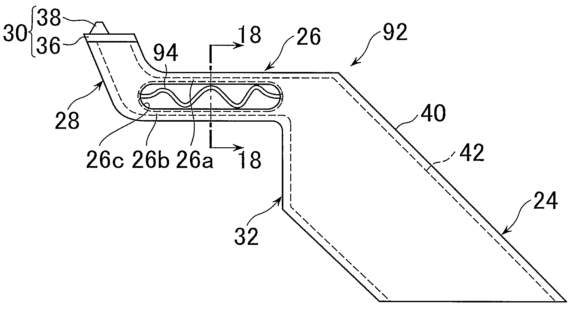
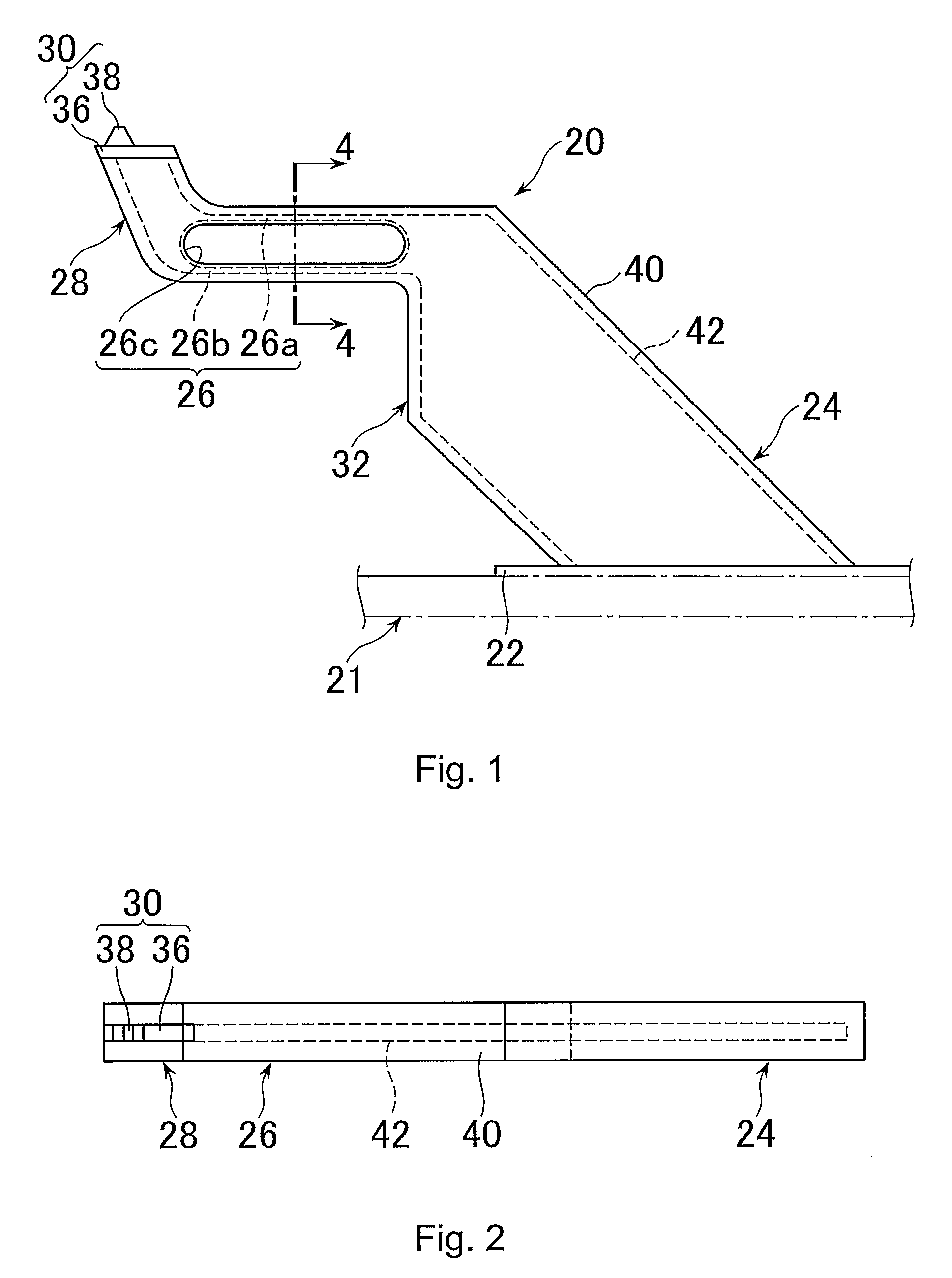
[0068]Hereinafter, in FIG. 1 which is shown to be upside down, the left-right direction is referred to as a left-right direction (first direction), the up-down direction is referred to as an up-down direction (second direction), and the direction perpendicular to the sheet is referred to as a front-back direction. These directions differ depending on the angle of a chuck top against the horizontal plane, the chuck top receives a device under test to which power is to be supplied. The device under test can be an integrated circuit (IC).

Embodiment of a Probe

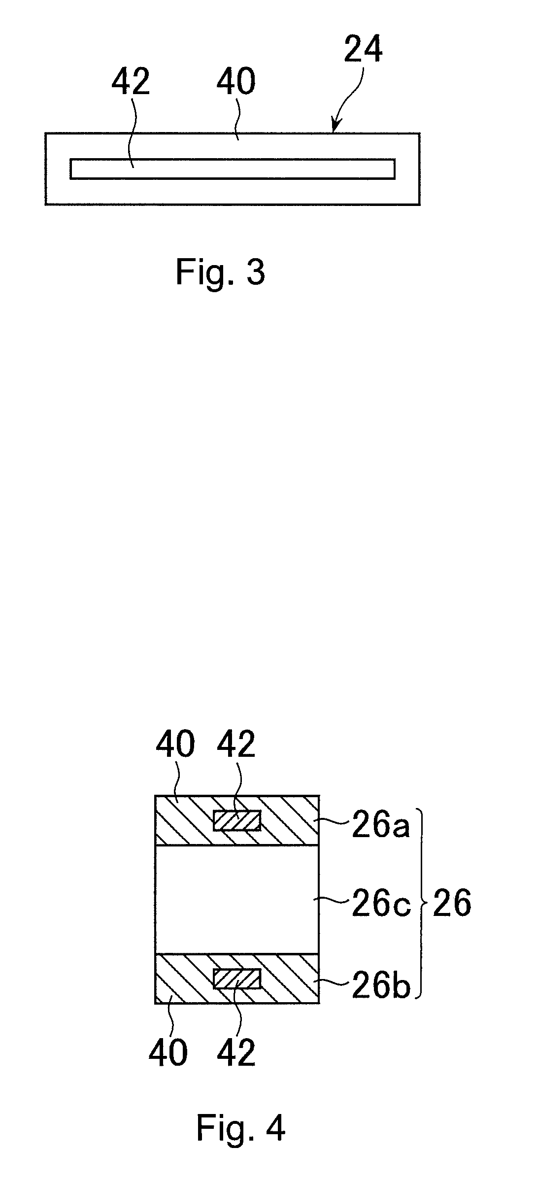
[0069]Referring to FIGS. 1 to 4, a probe 20 includes a plate-shaped seat region 24 to be attached to a connection land 22 of a support board 21 such as a wiring board or a ceramic board, a plate-shaped arm region 26 extending to one side in the left-right direction from the upper end portion of the seat region 24, a plate-shaped tip end region 28 protruded upward from the tip end of the arm region 26, and a probe tip portion or a p...


PUM


Abstract

A probe for electrical test comprises a plate-shaped main portion having a base end to be attached to a support board and a tip end opposite the base end, and a probe tip portion arranged at the tip end of the main portion and having a probe tip to contact an electrode of a device under test, the main portion being made of a tenacity material. The main portion includes a conductive material extending from the base end to the tip end and at least part of which is buried within the tenacity material, and the tenacity material has higher resiliency than that of the conductive material while the conductive material has higher conductivity than that of the tenacity material. As a result, disorder of a signal provided via the probe is decreased without losing elastic deformation.

Description

TECHNICAL FIELD[0001]The present invention relates to a probe for use in an electrical test of a flat-plate-shaped device under test such as a semiconductor integrated circuit.BACKGROUND ART[0002]A flat-plate-shaped device under test such as a semiconductor integrated circuit undergoes an electrical test to determine whether or not it is manufactured in accordance with the specification. The electrical test of this kind is performed by using an electrical connecting apparatus, such as a probe card, a probe block, a probe unit, or the like, having a plurality of probes (contactors) to be thrust to respective electrodes of the device under test. The electrical connecting apparatus of this kind is used to electrically connect the electrodes of the device under test to an electrical circuit, that is, a tester in an electrical test system.[0003]As an example of the probe to be used in the electrical connecting apparatus of this kind is raised a blade-type probe manufactured by using a so...

Claims


Application Information

Patent Timeline
Patent Type & Authority Patents(United States)
IPC IPC(8): G01R31/02
CPCG01R1/06727G01R1/06755G01R1/06733G01R1/073
Inventor HIRAKAWA, HIDEKISOMA, AKIRAHAYASHIZAKI, TAKAYUKIKUNIYOSHI, SHINJITAZAWA, MASAHISA
Owner NIHON MICRONICS
Why Eureka
Try Eureka