Input-capable display device

a display device and input technology, applied in the field of input-capable display devices, can solve the problems of complex system for generating a signal that removes noise, reduces the accuracy of detection of a position of contact, etc., and achieves the effect of suppressing the influence of nois

Active Publication Date: 2009-12-15
JAPAN DISPLAY WEST
View PDF6 Cites 47 Cited by
  • Summary
  • Abstract
  • Description
  • Claims
  • Application Information

AI Technical Summary

Benefits of technology

[0007]An advantage of some aspects of the invention is that it provides an input-capable display device, which is capable of suppressing an influence of noise without requiring a complex system.
[0010]In the input-capable display device according to the aspect of the invention, the shield conductor may be provided with a coated portion that constitutes a light shielding film. According to this aspect of the invention, because the shield conductor also serves as a light shielding film, the number of components is reduced and a manufacturing process is simplified.
[0011]In the input-capable display device according to the aspect of the invention, the shield conductor may be formed of a light reflective material. According to this aspect of the invention, by reflecting light that is blocked by the shield conductor among the rays of light entering the shield conductor, it is possible to suppress heating of the second substrate due to absorption of light.
[0012]In the input-capable display device according to the aspect of the invention, the shield conductor may be formed of a light absorption material. According to this aspect of the invention, by absorbing light that is blocked among the rays of light entering the shield conductor, it is possible to suppress a decrease in contrast due to reflection.

Problems solved by technology

In a liquid crystal display device with a touch panel function that uses the above electrostatic capacitance method, there is a problem that, when an electric field generated by a driving signal that is supplied between a pair of electrodes for driving a liquid crystal layer reaches the detection electrode, the accuracy of detection of a position of contact is decreased because this electric field component acts as a noise.
In the above existing liquid crystal display device with a touch panel function, however, the following problem still remains.
That is, in the existing liquid crystal display device with a touch panel function, there is a problem that it requires a complex system for generating a signal that removes a noise.

Method used


Image

  • Input-capable display device
  • Input-capable display device
  • Input-capable display device

Examples


first embodiment

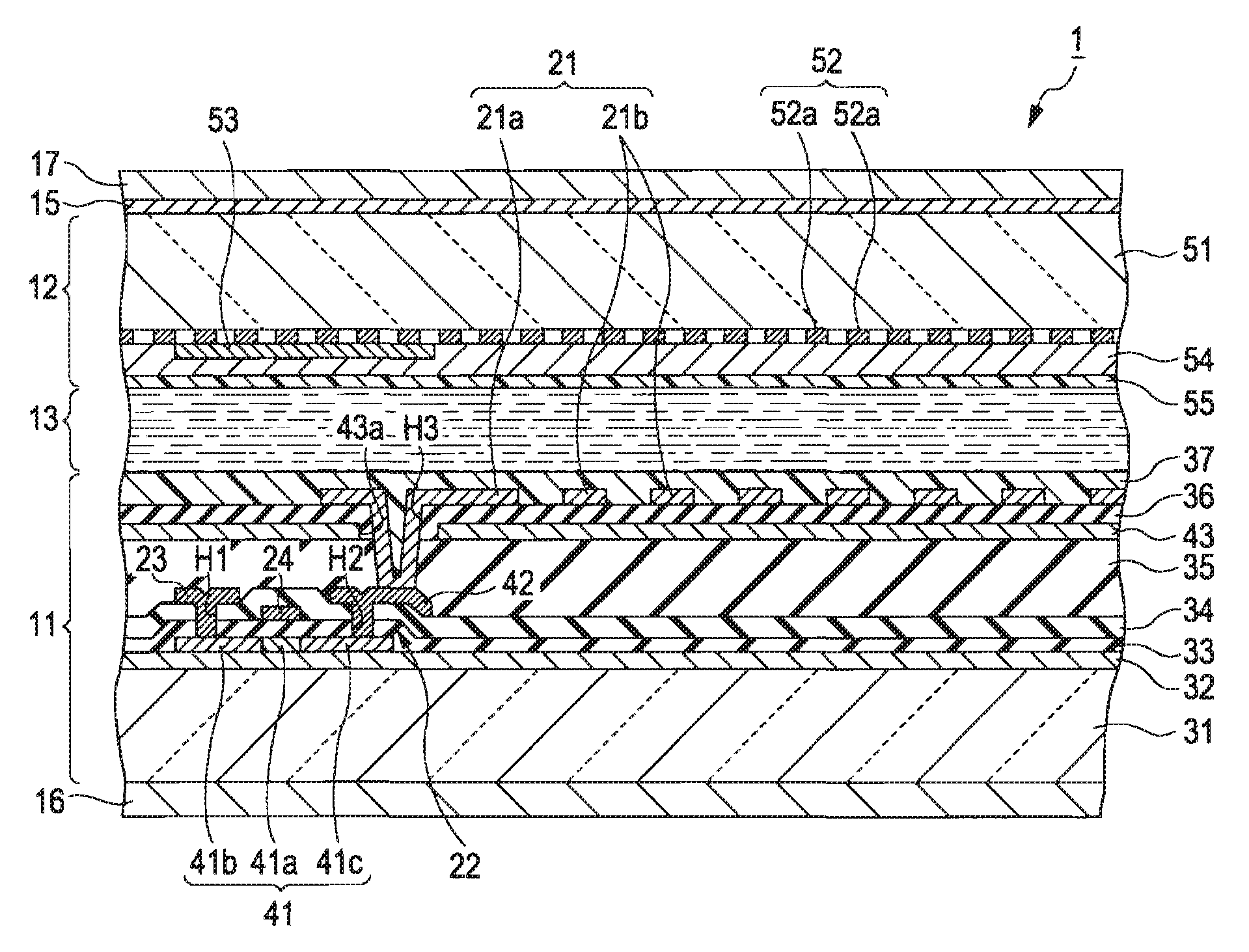
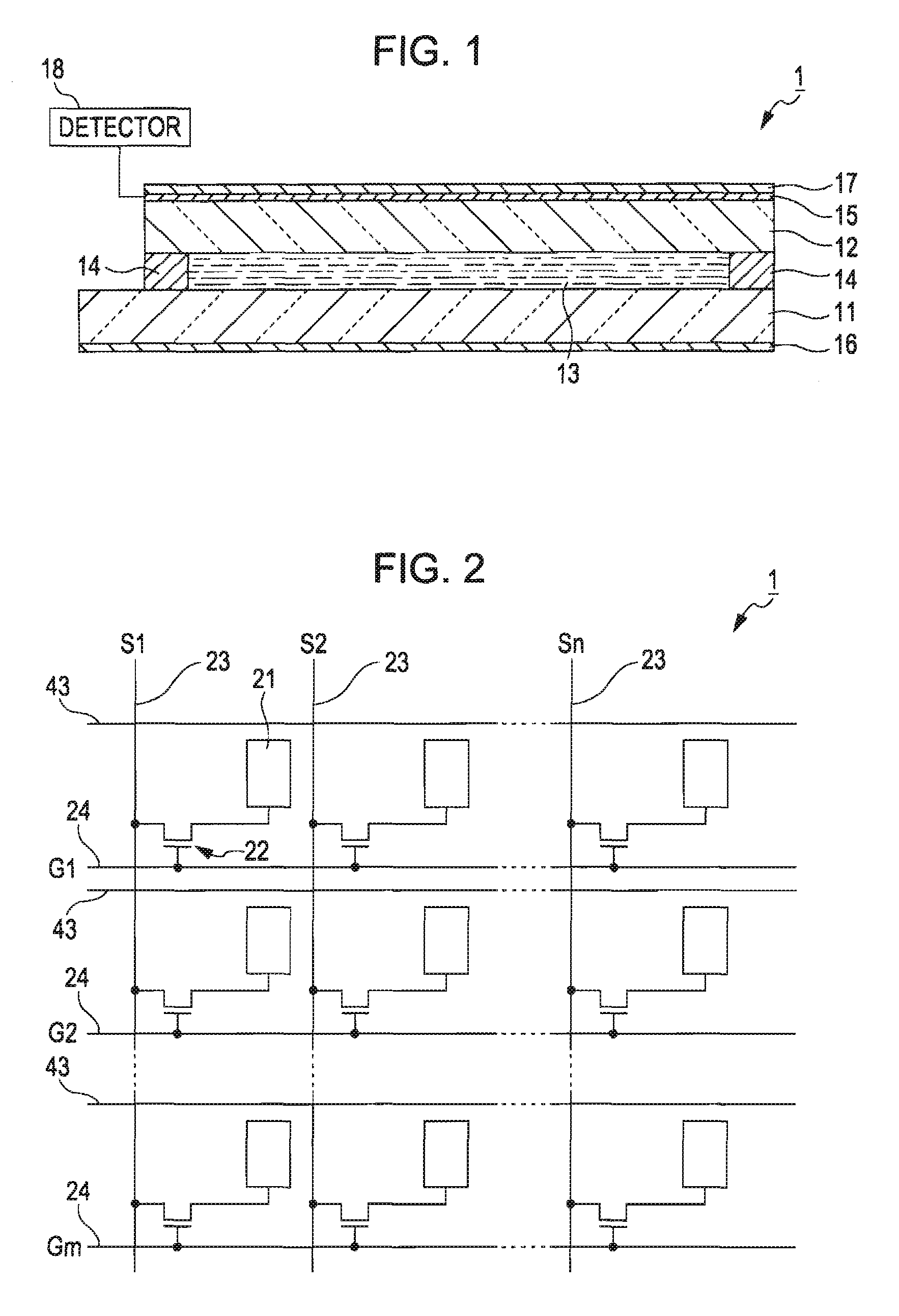
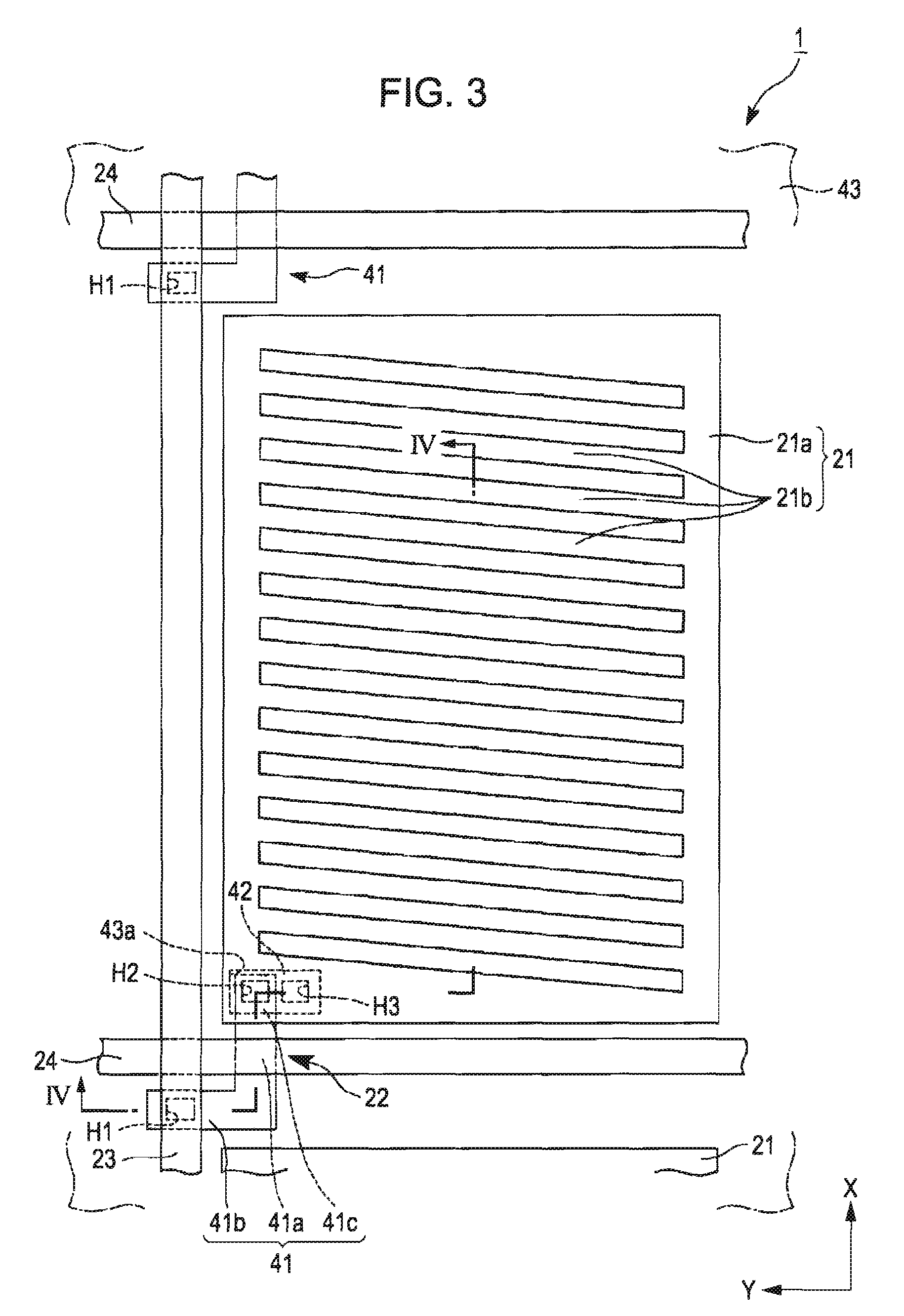
[0020]A first embodiment of an input-capable display device according to the invention will now be described with reference to the accompanying drawings. Note that the scales of the drawings used in the following description are appropriately changed in order to make the components be recognizable. Here, FIG. 1 is a schematic cross-sectional view that shows the input-capable liquid crystal display device. FIG. 2 is an equivalent circuit diagram of FIG. 1. FIG. 3 is a plan configuration diagram that shows a sub-pixel region. FIG. 4 is a cross-sectional view that is taken along the line IV-IV in FIG. 3.

Input-Capable Display Device

[0021]The input-capable liquid crystal display device (input-capable display device) 1 is a transmissive color liquid crystal display device, in which a single pixel is constituted of three sub-pixels that output colored rays of R (red), G (green), B (blue). Here, a display area that becomes a minimum unit for forming display's termed as “sub-pixel region”.

[0...

second embodiment

[0044]A second embodiment of an input-capable liquid crystal display device according to the invention will now be described with reference to the drawings. Here, FIG. 6 is a cross-sectional view that shows a sub pixel region. Note that, in the present embodiment, because the configuration of the sub-pixel region differs from that of the first embodiment, this point will be specifically described. The same reference numerals are assigned to the components described in the above embodiment, and a description thereof is omitted.

[0045]In the input-capable liquid crystal display device 110, as shown in FIG. 6, a shield electrode 112 that is provided in an opposite substrate 111 also serves as a light shielding film. That is, the opposite substrate 111 includes the substrate body 51, the shield electrode 112, the color filter layer 54 and the alignment layer 55. She shield electrode 112, the color filter layer 54 and the alignment layer 55 are sequentially laminated on the inner surface ...


PUM

PropertyMeasurementUnit
voltageaaaaaaaaaa
widthaaaaaaaaaa
widthaaaaaaaaaa

Abstract

An input-capable display device includes a first substrate a second substrate, a detection electrode, a dielectric film, and a detector. A pair of electrodes that drive a liquid crystal layer are provided on the first substrate. The second substrate is opposed to the first substrate through the liquid crystal layer. The detection electrode and the dielectric film are laminated on an outer surface of the second substrate. The detector detects a position at which an electrostatic capacitance is formed with the detection electrode through the dielectric film. The second substrate includes a shield conductor that is provided on a side adjacent to the liquid crystal layer. An electric potential of the shield conductor is fixed. The shield conductor has a plurality of birefringent structures that are arranged in a stripe.

Description

BACKGROUND[0001]1. Technical Field[0002]The present invention relates to an input-capable display device, such as, for example, a touch panel, to which an input function is added.[0003]2. Related Art[0004]In recent years, as a compact information electronic apparatus, such as a personal digital assistants (PDA) or a personal computer spreads, a display device that has added a so-called touch panel function, which is used for input operation by bringing an object, such as a finger or a pen, into contact with a display screen, has been widely used. In such a touch panel, there is an electrostatic capacitance method as a method for detecting a position at which a finger, or the like, contacts, which is, for example, described in Japanese Unexamined Patent Application Publication No. 2006-146895 and Japanese Unexamined Patent Application Publication No. 2003-196023. The electrostatic capacitance method is a method that flows a weak electric current through an electrostatic capacitance f...

Claims


Application Information

Patent Timeline
Patent Type & Authority Patents(United States)
IPC IPC(8): G02F1/1335G02F1/1343G06F3/044
CPCG06F3/044G06F3/0443G06F3/0412G02F1/13338G02F1/133528G02F1/13363G06F3/0445
Inventor UTSUNOMIYA, SUMIOKOSHIHARA, TAKESHIUSHIKI, TAKEYOSHIFUJIKAWA, YOICHI
Owner JAPAN DISPLAY WEST
Why Eureka
Try Eureka