Optical switch device and optical switching method

a technology of optical switch and optical switch, which is applied in the direction of optics, electrical appliances, instruments, etc., can solve the problems of loss of linearity of optical response, inability to increase the extinction ratio (the ratio of the maximum to the minimum intensity of transmitted light) and the likelihood of lowering the signal level

Inactive Publication Date: 2009-12-29
FUJITSU LTD
View PDF7 Cites 15 Cited by
  • Summary
  • Abstract
  • Description
  • Claims
  • Application Information

AI Technical Summary

Benefits of technology

[0023]The present invention is made in view of the above problems, and a first object of the present invention is to provide an optical switch device which adaptively controls the switch-output levels of time-division multiplexed optical pulses, and performs high-quality, flexible optical switching of the time-division multiplexed optical pulses.
[0024]In addition, a second object of the present invention is to provide an optical switching method which adaptively controls the switch-output levels of time-division multiplexed optical pulses, and performs high-quality, flexible optical switching of the time-division multiplexed optical pulses.

Problems solved by technology

The nonlinear optical effects are phenomena in which the properties of glass vary with the optical intensity of light which propagates through the glass, and the linearity of the optical response is lost when the power of the light is relatively strong.
On the other hand, in the waveguide switch, the insertion loss (the level loss occurring when light is inserted into the waveguide switch) occurs, and the extinction ratio (the ratio of the maximum to the minimum of the intensity of transmitted light) cannot be increased.
Therefore, in the waveguide switch, the signal level is likely to be lowered, and noise is likely to occur.
As described above, in the conventional optical switches such as the MEMS and the waveguide switch, the signal quality deteriorates.
In addition, the control of the optical switches based on electronic signal processing cannot realize high-speed switching.
Therefore, it is necessary to compensate for the differences among the optical levels at each receiver node, so that the convenience in system operation is deteriorated.
In addition, the numbers of channels of time-division multiplexed optical pulses of the signal light in the currently used systems are very large.
If, in such circumstances, the above optical amplifier for compensation for the differences among the optical levels is provided for every channel at each node in a network in which optical switching is performed, the equipment size and cost increase, and the increase in the equipment size and cost greatly impedes economical construction of an ultrafast optical communication network.

Method used


Image

  • Optical switch device and optical switching method
  • Optical switch device and optical switching method
  • Optical switch device and optical switching method

Examples


first embodiment

[0113]First, exemplary sequences of operations of the optical switch device are explained below.

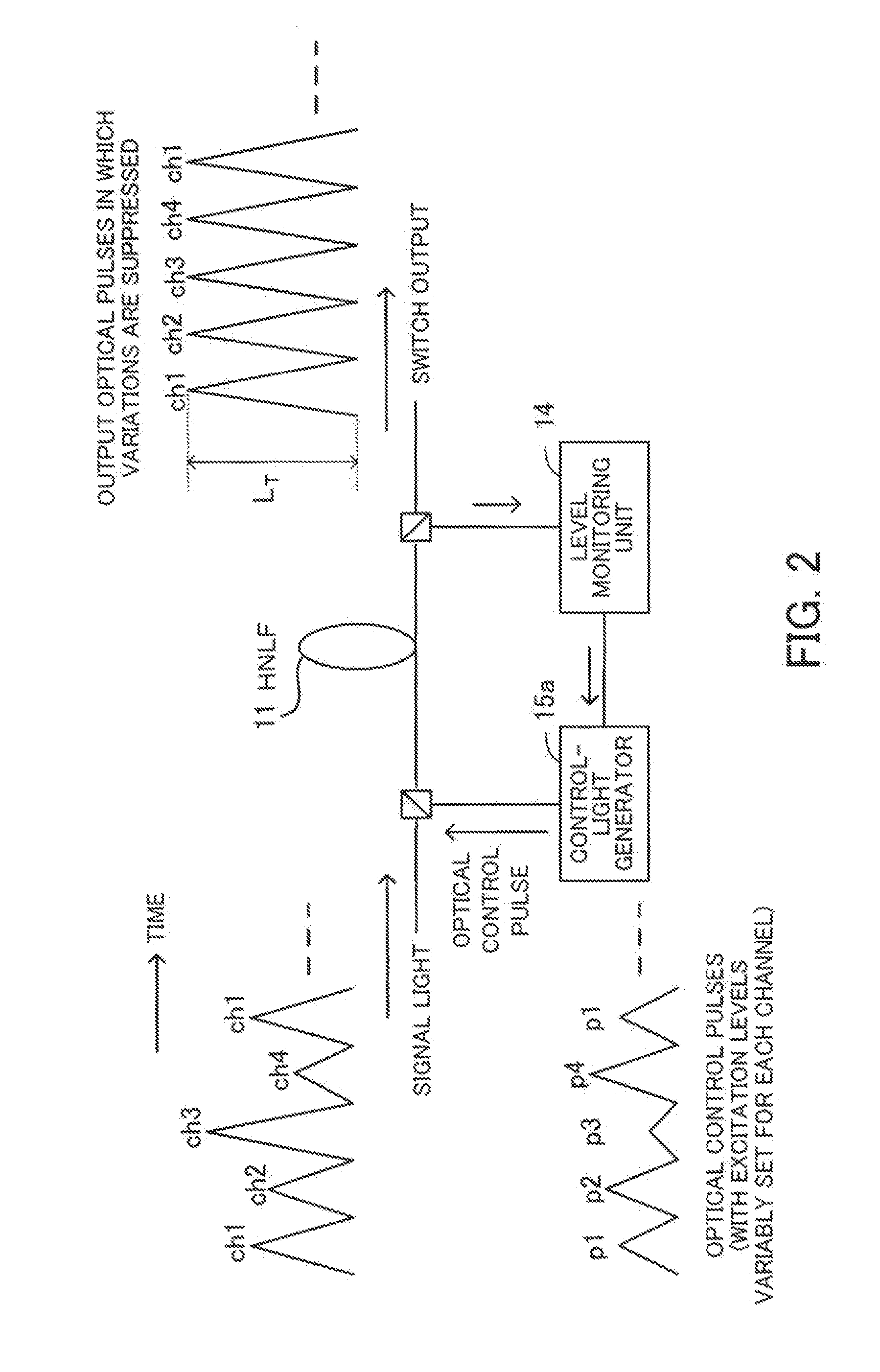
[0114]FIG. 7 is a flow diagram indicating a first exemplary sequence of operations of the optical switch device according to the first embodiment. The sequence of FIG. 7 also corresponds to the operations which are explained before with reference to FIG. 2.

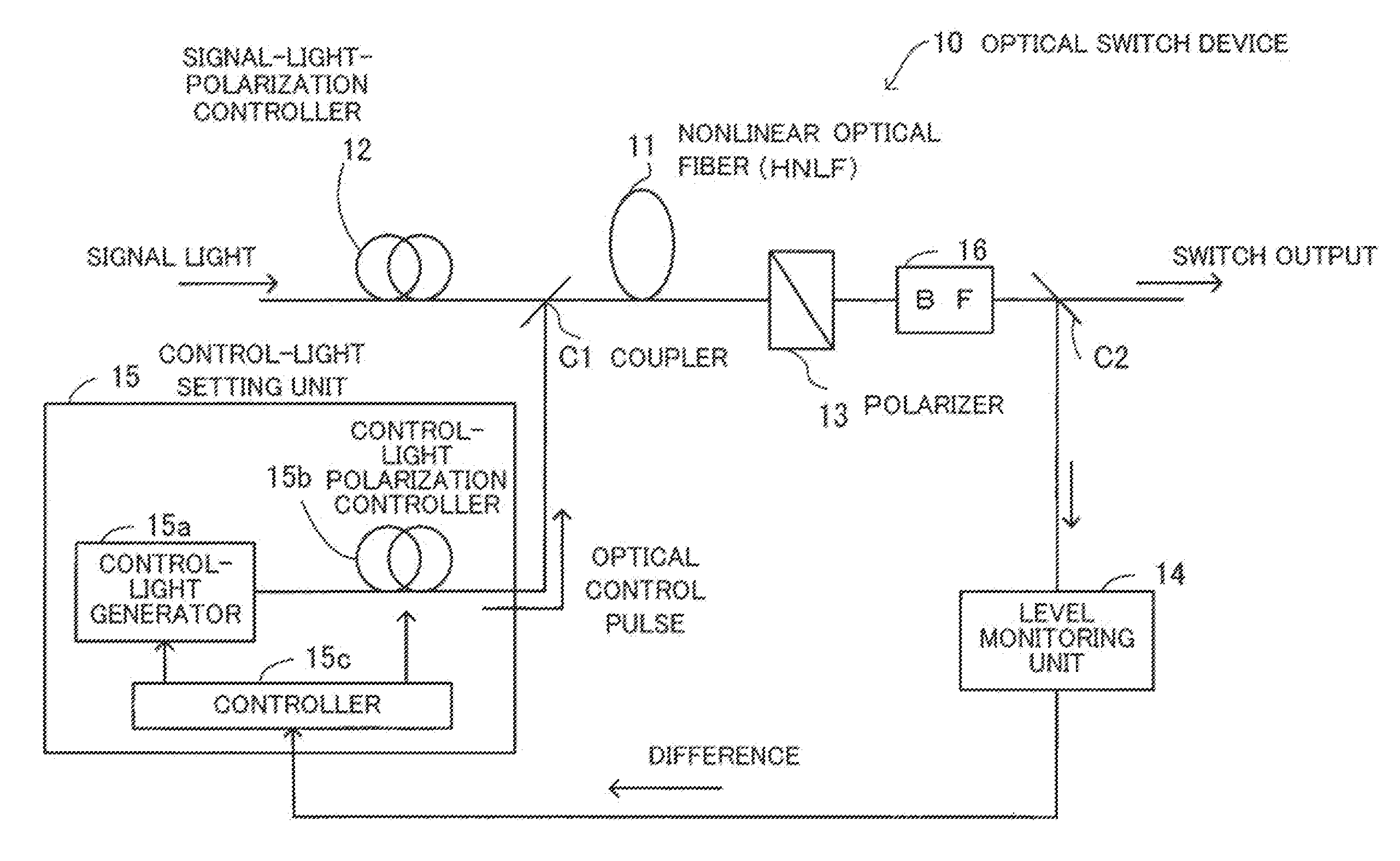
[0115]1> The control-light generator 15a generates optical control pulses p1 with their initial levels set to X1, and inputs the optical control pulses p1 into the HNLF 11 at the same timings as optical pulses of the signal light in the channel ch1. At this time, the levels of the optical control pulses p2 to p4 are set to zero.

[0116]2> The level monitoring unit 14 receives through the coupler C2 the optical pulses of the signal light in the channel ch1 outputted from the filter 16, performs opto-electric (O / E) conversion of the received optical pulses, and monitors the levels of the received optical pulses. When the monitored levels M...

second embodiment

[0143]Next, exemplary sequences of operations of the optical switch device are explained below.

[0144]According to the first embodiment, the levels of the optical control pulses for each channel are set in succession while the levels of the optical control pulses for the other channels (which may include one or more channels in which the levels of the optical control pulses are already set) are maintained at zero. That is, each channel is not in operation until the setting of the levels of the optical control pulses for all the channels is completed. On the other hand, according to the second embodiment, the levels of the optical control pulses for each channel are set in succession while one or more other channels in which the levels of the optical control pulses have already been set are in operation.

[0145]According to the second embodiment, first, the levels of the optical control pulses p1 in the channel ch1 (as a first one of the channels) are set so as to bring the output leve...

third embodiment

[0184]Hereinbelow, operations for controlling the levels of optical pulses outputted from the optical switch device are explained.

[0185]According to the third embodiment, a low-frequency signal is superimposed on optical control pulses so as to realize intensity modulation (amplitude modulation), and the intensity-modulated optical control pulses are inputted into the HNLF 11. Then, the levels of the optical control pulses for use in excitation in each channel are feedback controlled on the basis of the amplitude of a low-frequency signal superimposed on optical pulses which are intensity-modulated, switched, and outputted, so that the optical pulses outputted after switching are controlled at a desired level.

[0186]FIG. 13 is a diagram illustrating an outline of operations performed by the optical switch device according to the third embodiment of the present invention.

[0187]41> A superimposed signal p1a is generated by superimposing a low-frequency signal on optical control pulses...


PUM

PropertyMeasurementUnit
lengthaaaaaaaaaa
angleaaaaaaaaaa
rotation angleaaaaaaaaaa

Abstract

In an optical switch device, an optical control pulse is inputted into a nonlinear optical fiber in phase with each optical pulse of signal light which is to be outputted, so that the polarization directions of the optical control pulse and the signal light form a predetermined angle at the input stage of the nonlinear optical fiber, the optical control pulse causes polarization rotation and parametric amplification of the optical pulse in the nonlinear optical fiber, and then the optical pulse is outputted through a polarizer. The excitation level of the optical control pulse is set on the basis of the difference of a monitored output level of the optical pulse from a target level so that the output levels of optical pulses of the signal light are controlled at one or more desired levels.

Description

CROSS-REFERENCE TO RELATED APPLICATIONS[0001]This application is based upon and claims the benefits of priority from the prior Japanese Patent Application No. 2005-182424, filed on Jun. 22, 2005, the entire contents of which are incorporated herein by reference.BACKGROUND OF THE INVENTION[0002]1) Field of the Invention[0003]The present invention relates to an optical switch device and an optical switching method for switching optical signals.[0004]2) Description of the Related Art[0005]With the rapid expansion of the use of the Internet and the increase in the number of massive pieces of content, demands for communication networks having greater capacity and flexibility and realizing higher transmission speed have been increasing. In order to construct such communication networks, the optical communication technology is essential, and development and research of the optical communication are being performed in various fields.[0006]In particular, optical switches which perform on-off...

Claims


Application Information

Patent Timeline
Patent Type & Authority Patents(United States)
IPC IPC(8): H04J14/00G02F1/365
CPCG02F1/395G02F1/3515G02F1/0136G02F2001/392G02F1/392
Inventor TAMURA, YUJIWATANABE, SHIGEKI
Owner FUJITSU LTD
Why Eureka
Try Eureka