

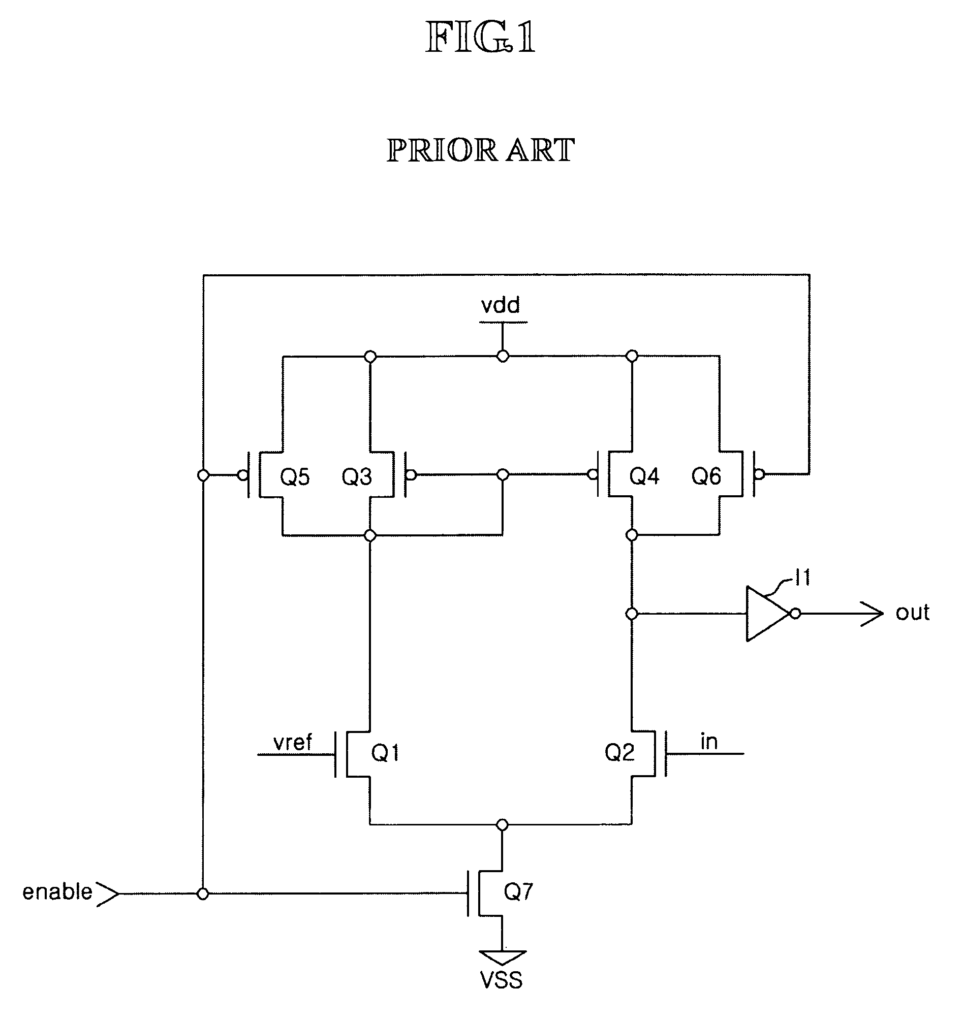
Input circuit for semiconductor integrated circuit
a technology of integrated circuits and input circuits, applied in logic circuit coupling/interface arrangements, instruments, pulse techniques, etc., can solve the problems of reduced setup/hold time margin and achieve the reduction of distortion of duty ratios, increase voltage gain, and increase signal swing width
- Summary
- Abstract
- Description
- Claims
- Application Information
AI Technical Summary
Benefits of technology
Problems solved by technology
Method used
Image

Examples
second embodiment
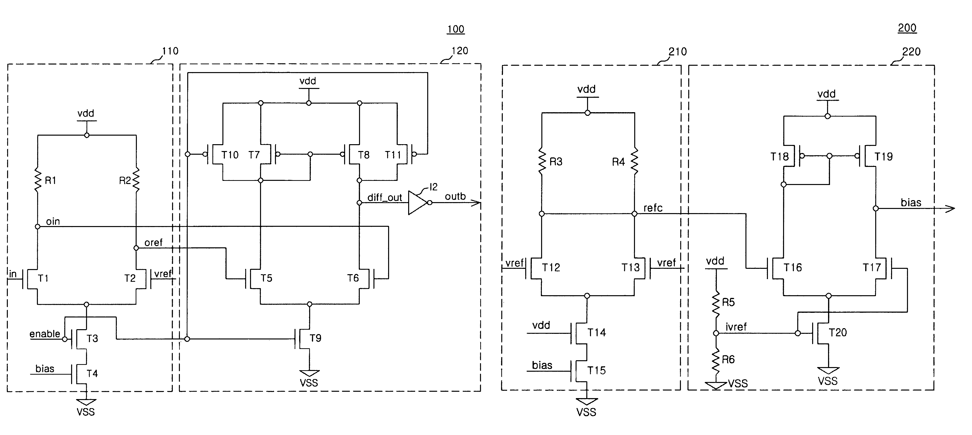
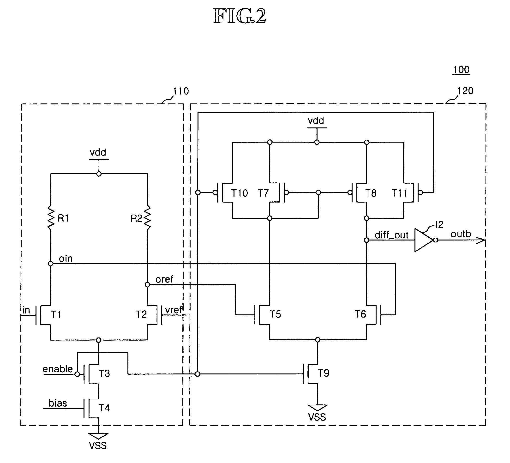
[0057]As described above, the input circuit for the semiconductor integrated circuit according to the present invention has two stages. If the enable signal enable is at a low level, the third transistor TR3 of the first input unit 310 is turned off, and the eleventh transistor TR11 of the second input unit 320 is turned off. Therefore, the input circuit does not perform an amplifying operation on the input signal in. At this time, since the seventh transistor TR7 is turned on, the final output signal out has a potential of a high level.
[0058]Meanwhile, if the enable signal is at a high level, the first input unit 310 and the second input unit 320 are activated, and perform an amplifying operation on the input signal in. The first input unit 310 amplifies the potential difference between the input signal in and the reference voltage Vref by a predetermined voltage gain, and outputs a result of the amplification. Also, the second input unit 320 amplifies the potential difference betw...
third embodiment
[0062]FIG. 5 is a diagram illustrating a structure of an input circuit for a semiconductor integrated circuit according to the invention.
[0063]An input circuit 400 for a semiconductor integrated circuit according to the third embodiment of the present invention may include a first input unit 310 and a second input unit 320a. The first input unit 310 may have the same structure as the first input unit 110 or 310 according to the above-described embodiments. Meanwhile, similar to the second input unit 320 according to the second embodiment of the invention, the second input unit 320a includes a pull-up unit 322a, a pull-up compensating unit 324, a pull-down unit 326a, and a pull-down compensating unit 328. The second input unit 320a according to still another embodiment of the present invention is different from the second input unit 320 in structures of the pull-up unit 322a and the pull-down unit 326a.
[0064]The pull-up unit 322a includes a fifth transistor TR5 that has one end (i.e...
PUM
 Abstract
Description
Claims
Application Information