Check patentability & draft patents in minutes with Patsnap Eureka AI!

Semiconductor memory device and control method thereof

a memory device and semiconductor technology, applied in the direction of memory adressing/allocation/relocation, digital storage, instruments, etc., can solve the problem that the device is not zbt-sram compatible, and achieve the effect of inhibiting a higher speed of the bus cycl

Inactive Publication Date: 2010-01-26
RENESAS ELECTRONICS CORP
View PDF23 Cites 24 Cited by
  • Summary
  • Abstract
  • Description
  • Claims
  • Application Information

AI Technical Summary

Benefits of technology

This solution eliminates wait times during refresh operations, enabling high-speed access compliant with QDR SRAM specifications by hiding the refresh operation within the cache memory system, thus allowing for faster and reliable concurrent read and write operations.

Problems solved by technology

The device, however, is not ZBT-SRAM compatible.

Method used


Image

  • Semiconductor memory device and control method thereof
  • Semiconductor memory device and control method thereof
  • Semiconductor memory device and control method thereof

Examples


Embodiment Construction

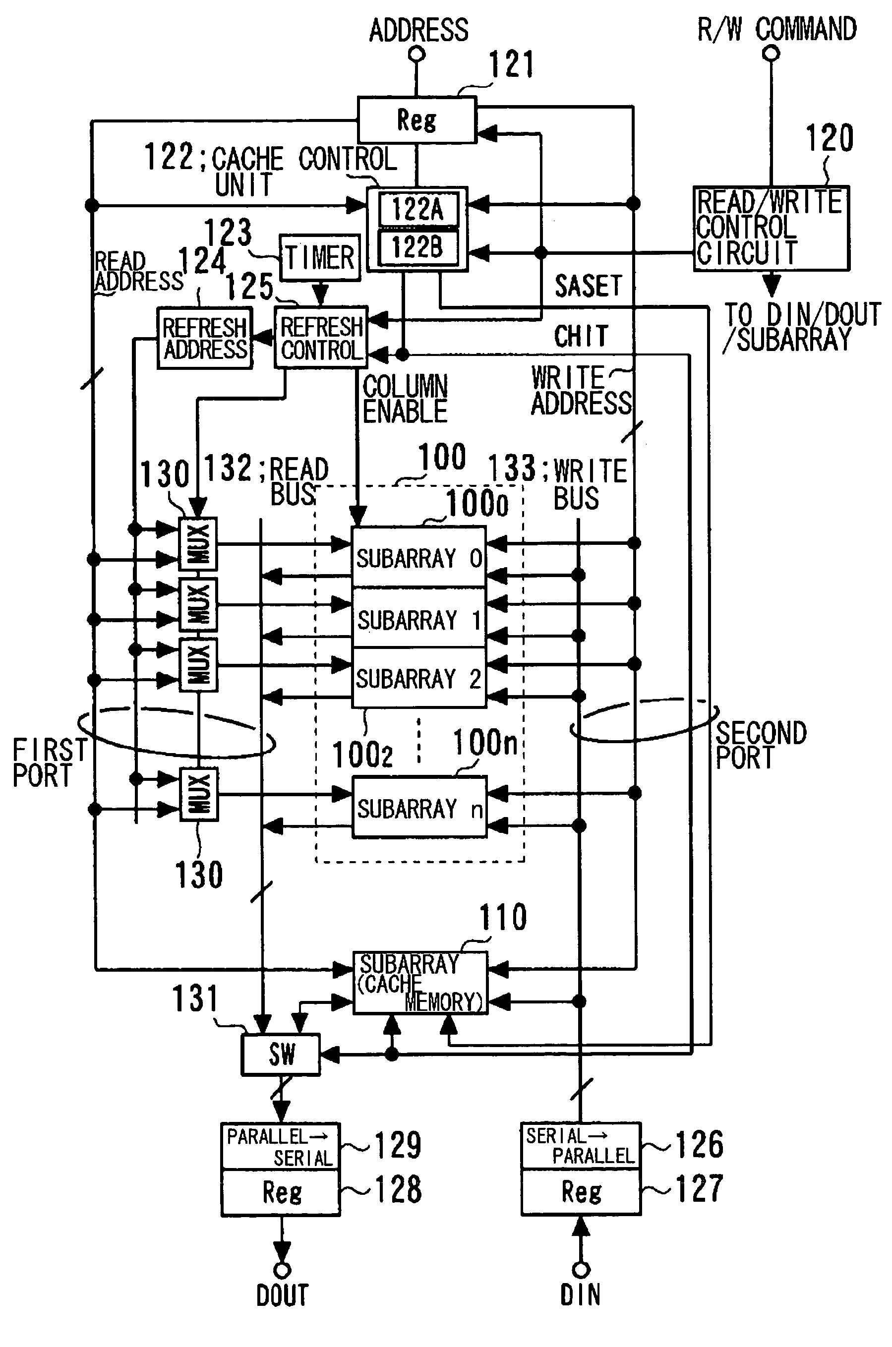
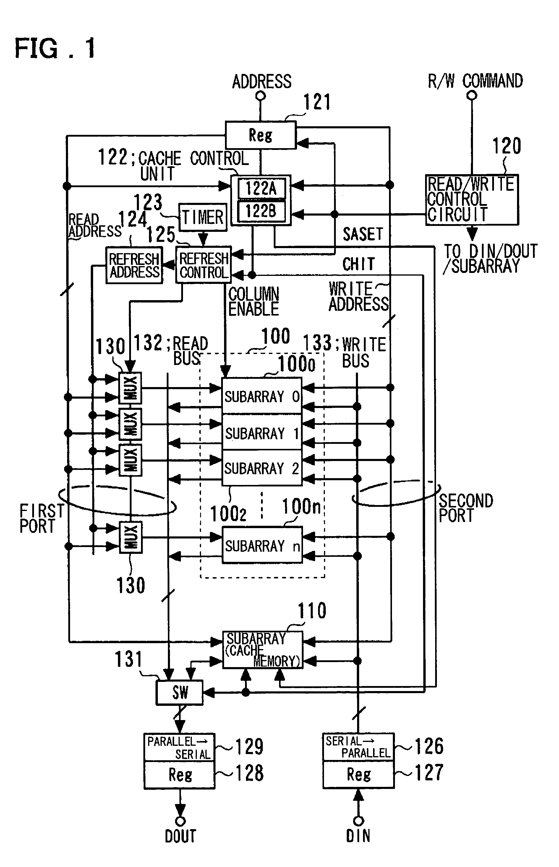
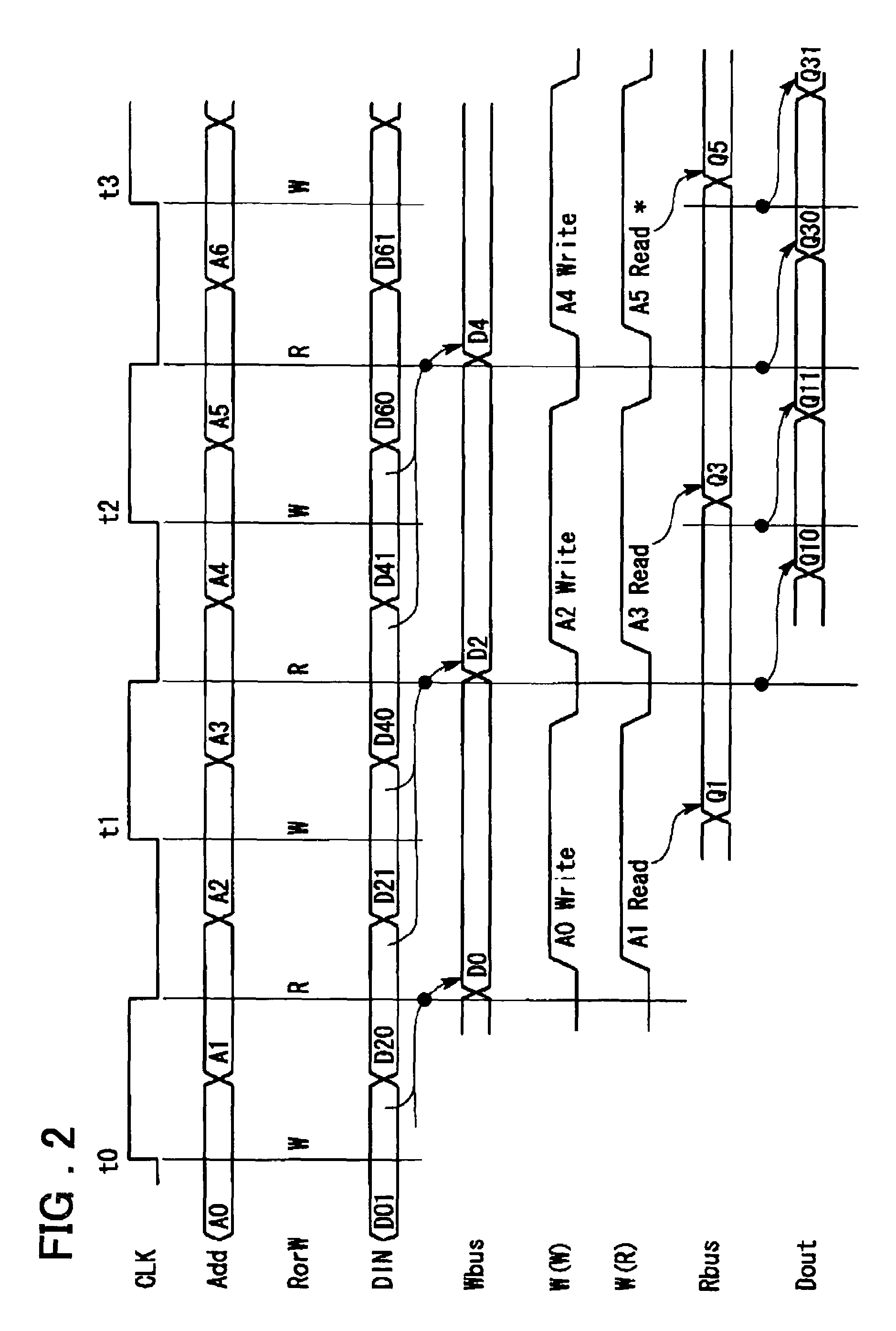
[0027]Embodiments of the present invention will be described in the below. In a semiconductor memory device compliant the QDR specification, a cell array is operated by a half clock in burst 2, and by one clock in burst 4. The cell array, comprised of plural DRAM cells each having two transistors, can be operated using a clock cycle twice of the cycle of a clock signal used for synchronization. Further, u sing a read-system port and a write-system port, read and write operations can be executed concurrently.

[0028]In one embodiment of the present invention, in order to hide a refresh, a cache memory is provided for the read-system port. Even if continuous accesses (alternate read and write accesses) to a sub-array, the sub-array is refreshed when a cache hits. With this arrangement, the present invention becomes compatible with the QDR SRAM specification.

[0029]In one embodiment of the present invention, as a measure for concurrently executing a read operation and a write operation at...


PUM


Abstract

A semiconductor memory device that does not delay read / write access due to a refresh and can be interface compatible with a high-speed SRAM such as a QDR SRAM, comprises a plurality of subarrays each having a plurality of dynamic memory cells; at least one cache memory for the plurality of subarrays; a circuit to check whether data read from the subarray selected by a read address is present in the cache memory or not; and a circuit performing control so that the check result indicates that the data is present in the cache memory, the data is read from the cache memory and refreshing of the subarray is performed concurrently with a read cycle.

Description

FIELD OF THE INVENTION[0001]The present invention relates to a semiconductor memory device. More specifically, the invention relates to a dynamic semiconductor memory device suitable for being applied to an SRAM semiconductor memory device and its control method.BACKGROUND OF THE INVENTION[0002]Quad Data Rate (QDR™) SRAM devices, which are high performance SRAMs used for communication applications and the like include separate data input and data output buses, and include separate / concurrent read and write ports. With respect to the latest information on the QDR SRAM, the following Nonpatent Document 1 and the like are referred to. QDR is a trademark of CYPRESS, HitaCHIT, IDT, Micron, NEC, and Samsung.[0003]While a DRAM (dynamic random access memory) device requires a periodic refresh operation and a pre-charge operation of a bit line, a SRAM device is excellent in terms of a data access cycle. On the other hand, in the SRAM device, each cell is composed by four transistors (two sel...

Claims


Application Information

Patent Timeline
Patent Type & Authority Patents(United States)
IPC IPC(8): G06F12/00G06F13/00G06F13/28G11C7/00G11C7/10G11C8/00G06F12/08G11C11/403G11C11/401G11C11/406
CPCG06F12/0893G11C7/1066G11C11/40615G11C11/406G06F2212/3042G11C2207/2245G11C2207/107
Inventor TAKAHASHI, HIROYUKI
Owner RENESAS ELECTRONICS CORP
Features
  • R&D
  • Intellectual Property
  • Life Sciences
  • Materials
  • Tech Scout
  • Unparalleled Data Quality
  • Higher Quality Content
  • 60% Fewer Hallucinations
Learn More