Plural light source and camera to detect surface flaws

a technology of surface flaws and light sources, applied in the field of systems and methods for detecting flaws in coated articles, can solve the problems of large flaws considered high frequency surface flaws, low frequency specular surface flaws, and large flaws

Inactive Publication Date: 2010-02-16
XEROX CORP
View PDF6 Cites 8 Cited by
  • Summary
  • Abstract
  • Description
  • Claims
  • Application Information

AI Technical Summary

Problems solved by technology

These coating defects in general are referred to as low frequency specular surface flaws due to the subtle nature of the change in coating thickness that accompanies these defects and to the mirror angle specular reflectance of light from these defects.
Larger flaws, which are also detrimental to producing clear images in the electrophotographic imaging process, are referred to as high frequency surface flaws.
Larger flaws are considered high frequency surface flaws.
Low frequency specular surface flaws and high frequency surface flaws detrimentally affect the performance of the OPC drum photoreceptor in reproducing images.
Flaws as small as about 1 μm can have a detrimental effect on the reproduced image.
This typically results in banding on the final image.
These methods, however, have proved not to be useful in detecting low frequency specular surface flaws on coated substrates.
This method is tedious, inefficient, costly, and time consuming.

Method used


Image

  • Plural light source and camera to detect surface flaws
  • Plural light source and camera to detect surface flaws
  • Plural light source and camera to detect surface flaws

Examples


Embodiment Construction

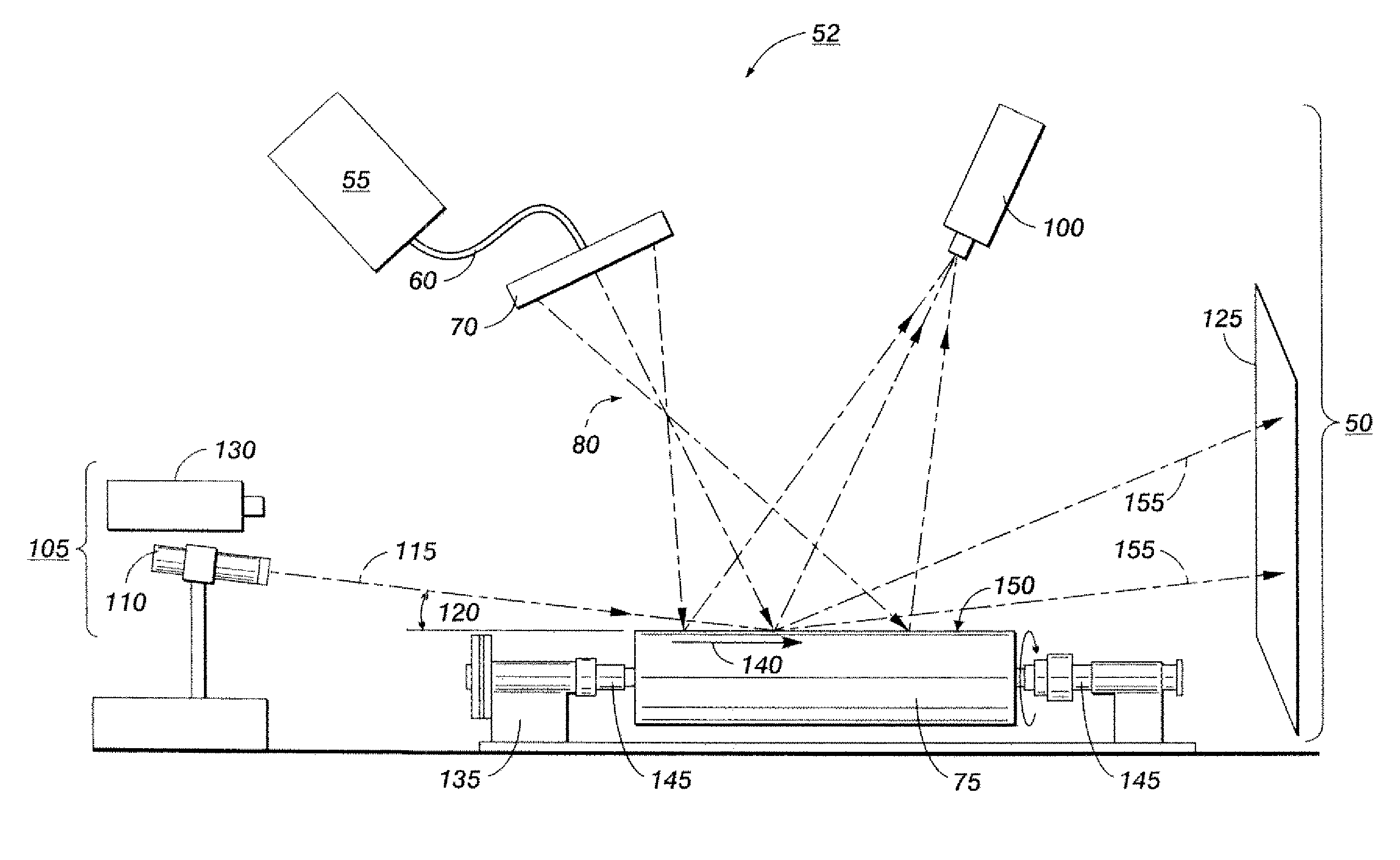
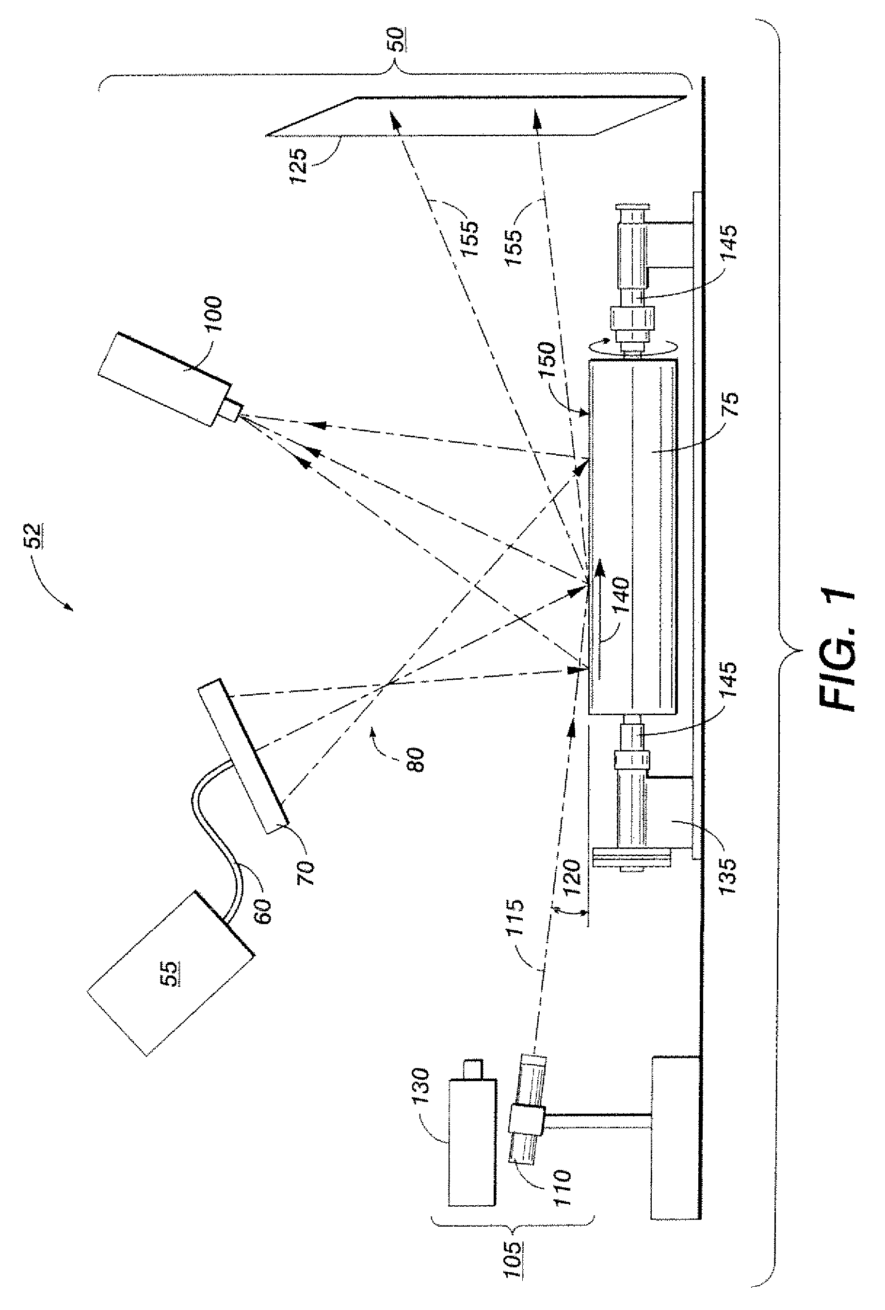
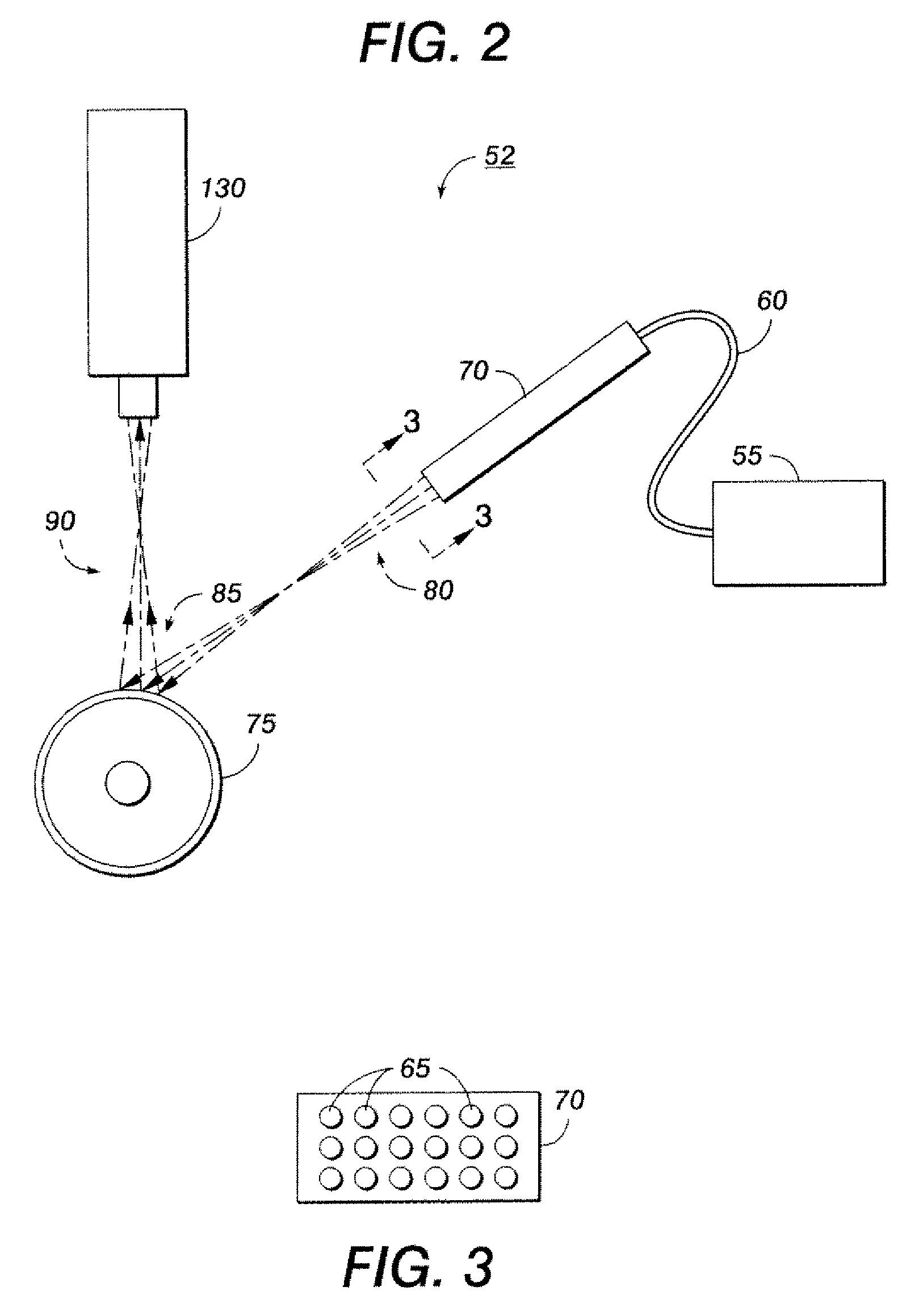
[0044]Before the present methods, systems and materials are described, it is to be understood that this disclosure is not limited to the particular methodologies, systems and materials described, as these may vary. It is also to be understood that the terminology used in the description is for the purpose of describing the particular versions or embodiments only, and is not intended to limit the scope. For example, as used herein and in the appended claims, the singular forms “a,”“an,” and “the” include plural references unless the context clearly dictates otherwise. In addition, the word “comprising” as used herein is intended to mean “including but not limited to.” Unless defined otherwise, all technical and scientific terms used herein have the same meanings as commonly understood by one of ordinary skill in the art. All of the patent publications mentioned herein are incorporated herein in their entireties. The optic terms “point sources”, “linear electromagnetic radiation sourc...


PUM

PropertyMeasurementUnit
standoff distanceaaaaaaaaaa
wavelengthaaaaaaaaaa
thicknessaaaaaaaaaa

Abstract

A method for detecting specular surface flaws on a coated substrate includes impinging visible non-integrated electromagnetic radiation from a first source onto the coated substrate, reflecting the visible non-integrated electromagnetic radiation off the coated substrate into a first photosensitive device, forming a recorded high frequency surface flaw image, and impinging visible coherent electromagnetic radiation from a second source onto a coated substrate at an oblique angle. The visible non-integrated electromagnetic radiation and the visible coherent electromagnetic radiation on the coated substrate are collocated but not combined on the substrate. The visible coherent electromagnetic radiation is reflected off the coated substrate onto a screen material to form a low frequency surface flaw image. The low frequency surface flaw image is recorded to form a recorded low frequency surface flaw image.

Description

CROSS-REFERENCE TO RELATED APPLICATIONS[0001]Not applicable.STATEMENT REGARDING FEDERALLY SPONSORED RESEARCH[0002]Not applicable.NAMES OF PARTIES TO A JOINT RESEARCH AGREEMENT[0003]Not applicable.SEQUENCE LISTING[0004]Not applicable.BACKGROUND[0005]1. Technical Field[0006]The disclosed embodiments generally relate to systems and methods for detecting flaws in coated articles.[0007]2. Description of the Related Art[0008]In the process of electrophotographic imaging, a photoconductive member is electrically charged to a uniform potential. The charged member is exposed to a light image of the original document. The light selectively discharges areas on the surface, while leaving other areas uncharged, thus producing an electrostatic latent image. A developer material, typically containing charged toner particles with opposite polarity as that of the photoconductive member, is brought into contact with the exposed photoconductive member. The charged toner particles are transferred to op...

Claims


Application Information

Patent Timeline
Patent Type & Authority Patents(United States)
IPC IPC(8): G01N21/00
CPCG01N21/8422G01N21/952
Inventor ZAMAN, KAMRAN UZPIETRZYKOWSKI, STANLEYPIETRANTONI, DANTEGOTTSCHALK, KENNETHSCHICHLER, RICHARD
Owner XEROX CORP
Why Eureka
Try Eureka