Semiconductor device and method for producing the same

a semiconductor device and semiconductor technology, applied in semiconductor devices, semiconductor/solid-state device details, electrical devices, etc., can solve the problems of reducing the thickness of the resin disposed in these portions, deteriorating an insulating property, and the size of the semiconductor device therefore increasing, so as to enhance the heat dissipation property and the effect of increasing the size of the semiconductor devi

Active Publication Date: 2010-03-02
MITSUBISHI ELECTRIC CORP
View PDF19 Cites 11 Cited by
  • Summary
  • Abstract
  • Description
  • Claims
  • Application Information

AI Technical Summary

Benefits of technology

[0008]On the other hand, the latter semiconductor device has a problem that since the coefficients of thermal expansion of the insulator and the resin are largely different, the insulator gets peeled off from the resin owing to heat generated by the power chips. Further, since an interface is created between the insulator and the resin, it is necessary to ensure a distance for creeping insulation to provide creeping insulation at this interface and the size of the semiconductor device therefore increases.
[0009]Accordingly, an object of the present invention is to provide a semiconductor device which exhibits an enhanced heat dissipation property, provides excellent insulation and can be reduced in size.

Problems solved by technology

While it is necessary for improvement in heat dissipation property that the resin covering the frames seating the power chips, namely, the resin between the back surfaces of the frames seating the power chips and the back surface of the semiconductor device is thin in the former semiconductor device, there is a problem that reduction in thickness of the resin disposed in these portions deteriorates an insulating property.
On the other hand, the latter semiconductor device has a problem that since the coefficients of thermal expansion of the insulator and the resin are largely different, the insulator gets peeled off from the resin owing to heat generated by the power chips.
Further, since an interface is created between the insulator and the resin, it is necessary to ensure a distance for creeping insulation to provide creeping insulation at this interface and the size of the semiconductor device therefore increases.

Method used


Image

  • Semiconductor device and method for producing the same
  • Semiconductor device and method for producing the same
  • Semiconductor device and method for producing the same

Examples


embodiment 1

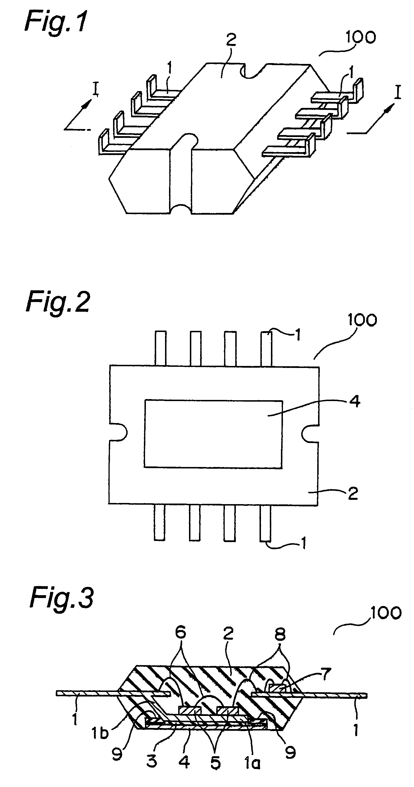
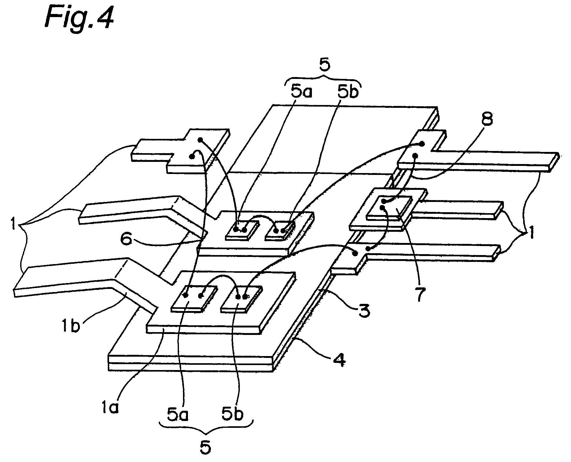
[0021]FIG. 1 is a perspective view of a semiconductor device according to this embodiment of the present invention generally denoted at 100. FIG. 2 is a back surface view of the semiconductor device 100 of FIG. 1 while FIG. 3 is a cross sectional view of the semiconductor device 100 of FIG. 1, both taken along the direction I-I. FIG. 4 is a perspective view which shows a portion inside the semiconductor device 100 of FIG. 1.

[0022]As shown in FIG. 1, the semiconductor device 100 has a resin-molded package structure and includes a mold resin 2 on the both sides of which a plurality of metal frames 1 are disposed. The mold resin 2 is preferably of an epoxy resin.

[0023]As shown in FIG. 2, to the back surface of the mold resin 2, an insulation resin sheet 3 is disposed whose back surface seats a metal foil 4 of copper for instance. The insulation resin sheet 3 is preferably of an epoxy resin containing fillers. The fillers are made of one or materials selected from Sio2, Al2O3, AlN, Si3N...

embodiment 2

[0056]FIG. 7 is a cross sectional view of a semiconductor device according to this embodiment of the present invention generally denoted at 200. FIG. 7 is a cross sectional view taken along the same direction as the direction I-I shown in FIG. 1. In FIG. 7, the same reference symbols as those in FIGS. 1-3 denote the same or corresponding portions.

[0057]In the semiconductor device 200 according to the embodiment 2, the resin sheet 3 seating the metal foil 4 has such a size which covers the entire back surface of the mold resin 2. The semiconductor device is otherwise the same in structure as the semiconductor device 100 described above.

[0058]The semiconductor device 200 exhibits an enhanced heat dissipation property, and does not require positioning of the resin sheet 3 at the producing steps (the step 4 described above). In other words, since the resin sheet 3 has the same size as that of an inner bottom surface of the resin-sealing metal mold 20, it is not necessary to precisely co...

embodiment 3

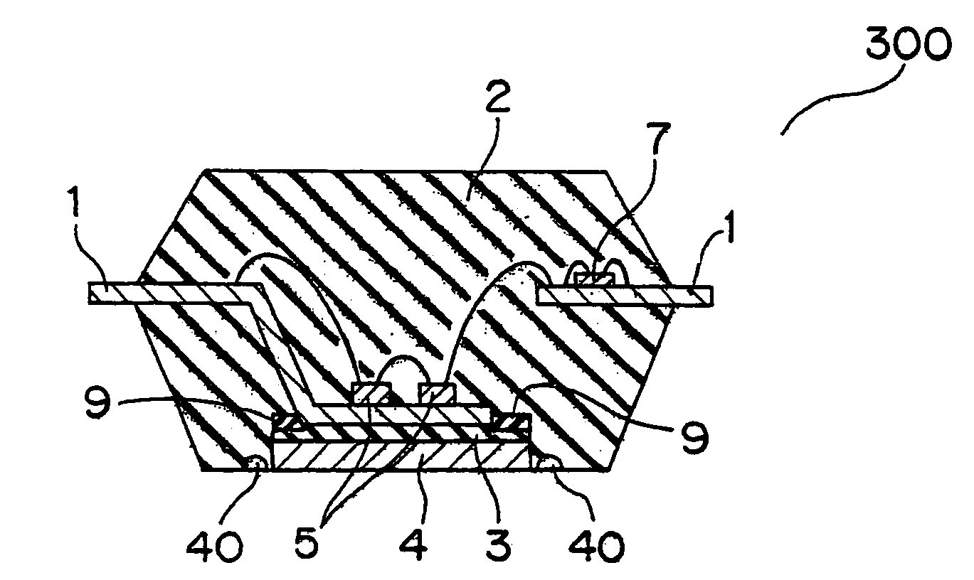
[0059]FIG. 8 is a back surface view of a semiconductor device according to this embodiment of the present invention generally denoted at 300. FIG. 9 is a cross sectional view taken along the direction IIIV-IIIV of FIG. 8. In FIGS. 8 and 9, the same reference symbols as those in FIGS. 1-3 denote the same or corresponding portions.

[0060]The semiconductor device 300 includes a plurality of concave portions 40 around the sheet resin 3. Further, screw holes 35 are formed which are for attaching a cooling fin (not shown).

[0061]The concave portions 40 are created in the resin sheet 3 as a plurality of projections (not shown) are formed in the inner bottom surface of the metal mold 20 at the step 4 described above (FIG. 5D) for the purpose of making the positioning easy. In the inner bottom surface of the metal mold 20, the projections are disposed along the area where the resin sheet 3 is disposed.

[0062]The projections disposed in the inner bottom surface of the metal mold 20 thus makes th...


PUM


Abstract

A semiconductor device in which chips are resin-molded, including: frames having front and back surfaces and die pads; power chips mounted on the surfaces of the die pads; an insulation resin sheet having a first and a second surfaces which are opposed against each other, the resin sheet being disposed such that the back surfaces of the die pads contact the first surface of the resin sheet; and a mold resin applied on the first surface of the resin sheet so as to seal up the power chips. The thermal conductivity of the resin sheet is larger than that of the mold resin.

Description

CROSS-REFERENCE TO RELATED APPLICATION[0001]The disclosure of Japanese Patent Application No. 2003-339730 filed on Sep. 30, 2003 including specification, drawings and claims is incorporated herein by reference in its entiretyBACKGROUND OF THE INVENTION[0002]1. Field of the Invention[0003]The present invention relates to a semiconductor device, and more particularly, a power semiconductor device including a power chip.[0004]2. Description of the Related Art[0005]In a conventional power semiconductor device, a power chip, an IC chip and the like are each die-bonded on a frame and these chips are sealed with a resin. Since a power chip has large heat dissipation, a cooling fin is attached to the back surface of the semiconductor device for instance to thereby enhance a heat dissipation efficiency. The frames seating the power chips are coated with a resin and insulated from the cooling fin which is attached to the back surface (e.g., JP 2000-138343, A).[0006]Meanwhile, such a semicondu...

Claims


Application Information

Patent Timeline
Patent Type & Authority Patents(United States)
IPC IPC(8): H01L23/495H01L23/28H01L23/29H01L21/56H01L23/36H01L23/433H01L23/50
CPCH01L21/565H01L23/4334H01L23/49575H01L2224/48091H01L2224/48137H01L2224/48247H01L2924/01079H01L2924/13055H01L2924/14H01L2924/00014H01L24/48H01L2224/45124H01L2224/45144H01L2924/00H01L2224/45015H01L24/45H01L2924/181H01L2224/49113H01L24/49H01L2224/05599H01L2924/00012H01L23/28H01L21/56H01L23/36
Inventor HAYASHI, KENICHIKAWAFUJI, HISASHITAKESHITA, TATSUYUKIFUNAKOSHI, NOBUHITOOZAKI, HIROYUKITADA, KAZUHIRO
Owner MITSUBISHI ELECTRIC CORP
Why Eureka
Try Eureka