Optical device, exposure apparatus, and device manufacturing method

a technology of exposure apparatus and exposure device, which is applied in the direction of mountings, printing, instruments, etc., can solve the problems of reducing the performance of the optical system, reducing the adhesive force and the elastic force, and achieving the effect of limiting the incidence of ligh

Active Publication Date: 2010-03-02
CANON KK
View PDF9 Cites 12 Cited by
  • Summary
  • Abstract
  • Description
  • Claims
  • Application Information

AI Technical Summary

Benefits of technology

[0007]The present invention has been made in consideration of the above-described problem, and has as its object to more effectively limit light incidence on, e.g., an adhesive material fixing an optical element.
[0010]According to the present invention, it is possible to more effectively limit light incidence on, e.g., an adhesive material fixing an optical element.

Problems solved by technology

Upon being irradiated with light (typically, ultraviolet rays), the adhesive material connecting the optical element to the supporting member deteriorates, which can result in a decrease in adhesive force and a change in elastic force.
This can change the position, orientation, and shape of the optical element, and can therefore decrease the performance of the optical system.

Method used


Image

  • Optical device, exposure apparatus, and device manufacturing method
  • Optical device, exposure apparatus, and device manufacturing method
  • Optical device, exposure apparatus, and device manufacturing method

Examples


first embodiment

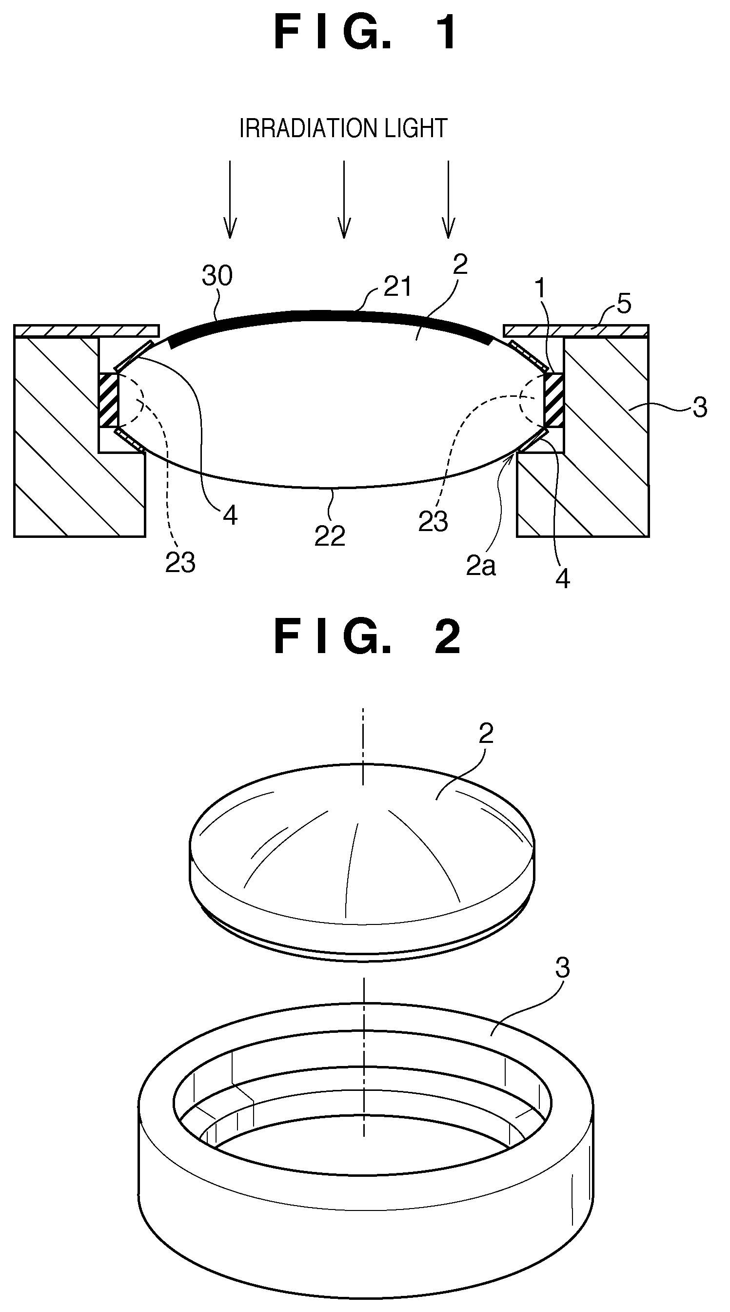
[0020]FIG. 1 shows the schematic arrangement of an optical device according to the first embodiment of the present invention. The optical device according to the first embodiment comprises an optical element 2, a supporting member 3 which is connected to a part 23 of the optical element 2 through an adhesive material 1 and supports the optical element 2, and a light shielding film 4 formed on the surface of the optical element 2 to limit light incidence on the adhesive material 1.

[0021]An example of the optical element 2 is a lens. The part 23 of the optical element 2 is typically at least a part of the side portion of the optical element 2. The light shielding film 4 can be formed on the surface of the optical element 2 by, e.g., coating. Referring to FIG. 1, irradiation light enters the optical element 2 from its upper surface side (to be referred to as an object side hereinafter). The irradiation light irradiates an irradiated region 30 on an object side surface 21 of the optical...

second embodiment

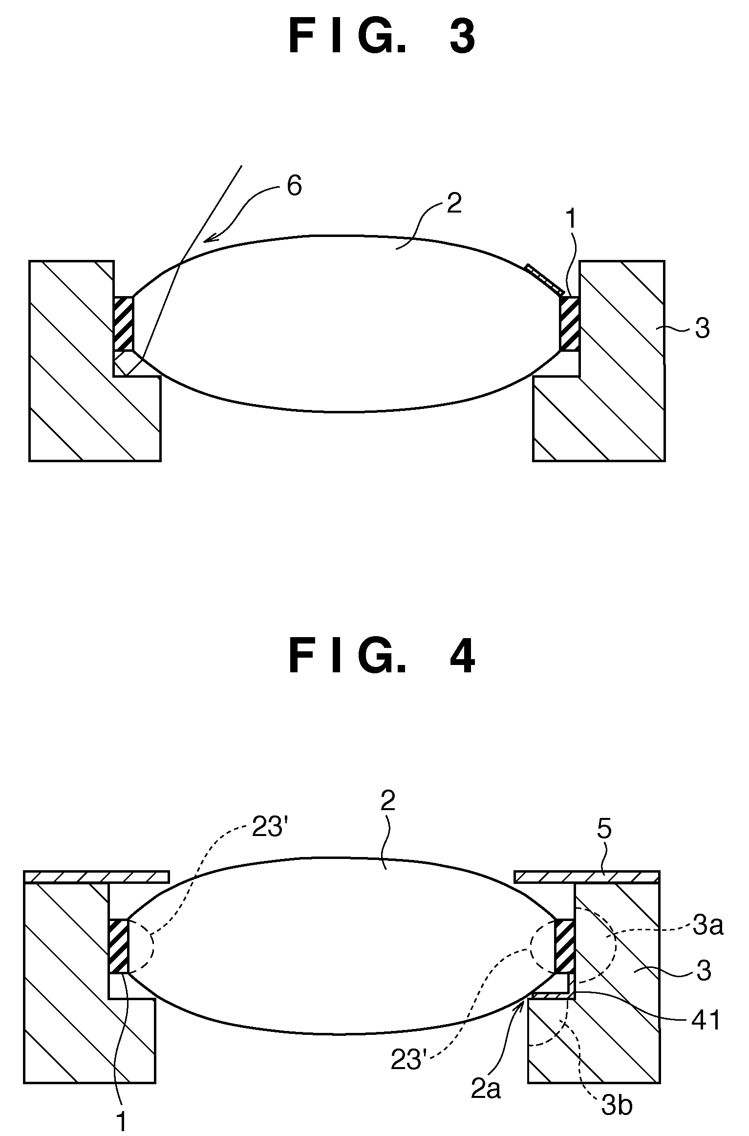
[0026]FIG. 4 shows the schematic arrangement of an optical device according to the second embodiment of the present invention. The optical device according to the second embodiment comprises an optical element 2, a supporting member 3 which is connected to at least a part 23′ of the side portion of the optical element 2 through an adhesive material 1 and supports the optical element 2, and an incidence limiting portion 41 which limits light incidence on the adhesive material 1. An example of the optical element 2 is a lens.

[0027]The supporting member 3 comprises a first supporting portion 3a which is connected to at least the part 23′ of the side portion of the optical element 2 through the adhesive material 1, and a second supporting portion 3b which supports the peripheral portion of the optical element 2 from below. The incidence limiting portion 41 is inserted between the contact portion between the adhesive material 1 and the first supporting portion 3a and a contact portion 2a...

third embodiment

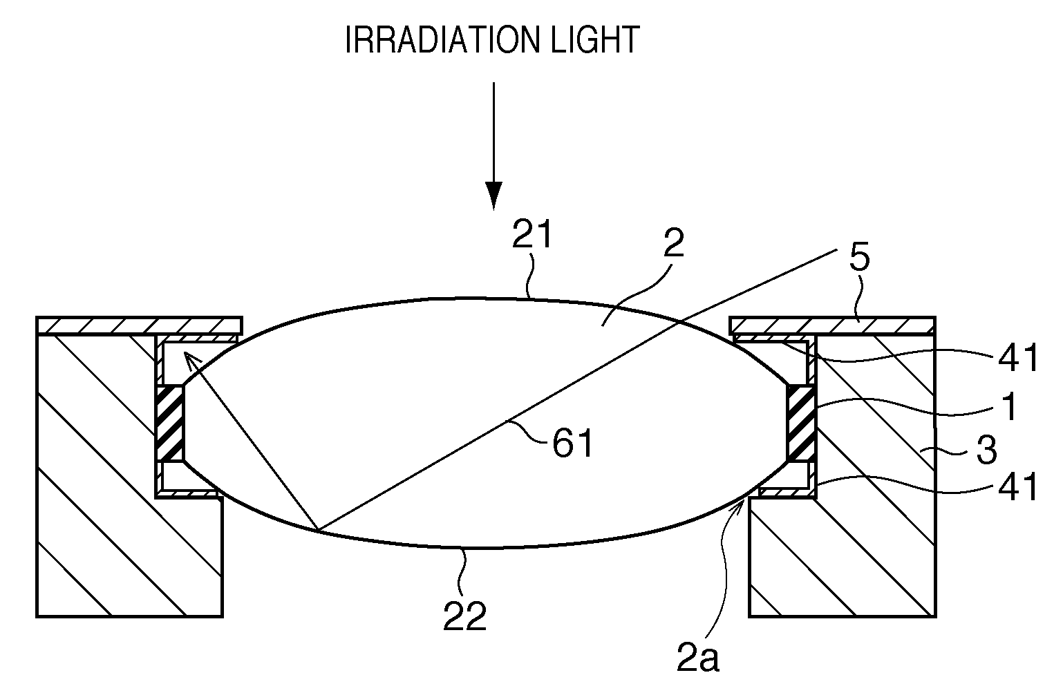
[0029]FIG. 5 shows the schematic arrangement of an optical device according to the third embodiment of the present invention. The third embodiment is different from the second embodiment in that an incidence limiting portion 41 is additionally provided on a side opposite to a second supporting portion 3b with respect to an adhesive material 1. A description of the same parts as those in the above-described embodiments will not be repeated. As shown in FIG. 5, a light beam 61 which has been generated by scattered light and has entered an optical element 2 can enter the adhesive material 1 upon being reflected by an image side surface 22 of the optical element 2 and further reflected by a light shielding member 5. To avoid this situation, the incidence limiting portions 41 are provided on the surface of the light shielding member 5 on the side of the adhesive material 1 and on the surface of a supporting member 3 from the adhesive material 1 to the light shielding member 5, as shown i...


PUM


Abstract

This invention effectively limits light incidence on an adhesive material fixing an optical element. An optical device includes an optical element, a supporting member connected to the optical element through an adhesive material to support the optical element, and a light shielding film formed in an unirradiated region on the surface of the optical element to limit light incidence on the adhesive material.

Description

BACKGROUND OF THE INVENTION[0001]1. Field of the Invention[0002]The present invention relates to an optical device, an exposure apparatus including the optical device, and a device manufacturing method using the exposure apparatus.[0003]2. Description of the Related Art[0004]An exposure apparatus is used in lithography for manufacturing a device such as a semiconductor device. The exposure apparatus illuminates an original by an illumination optical system, and projects the pattern of the original onto a substrate via a projection optical system, thereby exposing the substrate. An adhesive material is used to fix an optical element on a supporting member in an optical system such as an illumination optical system and projection optical system.[0005]FIGS. 2 and 3 schematically show a partial arrangement of an optical system such as an illumination optical system and projection optical system of an exposure apparatus. An optical element (e.g., a lens or mirror) 2 of the optical system...

Claims


Application Information

Patent Timeline
Patent Type & Authority Patents(United States)
IPC IPC(8): G02B7/02
CPCG03B27/72G03F7/70825G03F7/70958
Inventor KAWANAMI, KENTAROU
Owner CANON KK
Why Eureka
Try Eureka