Parallel-plate electrode reactor having an inductive antenna coupling power through a parallel plate electrode

a parallel plate electrode and reactor technology, applied in the field of plasma reactors, can solve the problems of inferior etch selectivity and etch profile, inability to provide independent control of ion density and ion energy, and material such as aluminum oxide tend to produce greater contamination

Inactive Publication Date: 2002-03-26
APPLIED MATERIALS INC
View PDF47 Cites 45 Cited by
  • Summary
  • Abstract
  • Description
  • Claims
  • Application Information

AI Technical Summary

Problems solved by technology

In contrast, capacitively coupled reactors typically provide relatively lower plasma ion densities (e.g., on the order of only 10.sup.10 ions / cm.sup.3) and generally cannot provide independent control of ion density and ion energy.
In contrast, parallel plate capacitively coupled plasma reactors typically stop etching at feature sizes on the order of about 0.25 microns, or at least exhibit inferior etch selectivity and etch profile due to an inferior ion-to-neutral density ratio.
However other materials such as aluminum oxide tend produce greater contamination than quartz due to sputtering.
However, the side wall is a poor ground plane, as it has many discontinuities, such as a slit valve for wafer ingress and egress, gas distribution ports or apparatus and so forth.
Such discontinuities give rise to non-uniform current distribution, which distort plasma ion distribution relative to the wafer surface.
The resulting sideways current flow toward the side wall contributes to non-uniform plasma ion distribution relative to the wafer surface.
The main problem with this type of plasma reactor is that it is liable to exhibit processing non-uniformity across the wafer surface.
The etch process near the wafer center is dependent upon such energetic electrons traveling from the vicinity of the chamber side wall and reaching the wafer center before recombining along the way by collisions with neutral species or ions, so that the etch process is not uniform across the wafer surface.
Moreover, introduction of the etchant precursor gas from the side and coupling of plasma source power from the side produces a non-uniform etchant ion / radical distribution favoring the side.
Many of the ions and radicals formed near side (over the wafer periphery) are consumed by etching the quartz side wall and are not available to etch the wafer center, while etchant ion / radical-forming energetic electrons generated near the side are lost to collisions with other species before reaching the wafer center, thus reducing the etchant ion concentration at the wafer center.
(It should be noted that the etching of the quartz side wall greatly increases the cost of operating the reactor because it consumes a very expensive item--the quartz side wall, which must be periodically replaced.)
The converse of the foregoing is that the relative plentitude of etchant ions and radicals near the wafer periphery can, under selected processing conditions, so impede polymerization as to impair etch selectivity, possibly leading to punchthrough of the underlying layer near the wafer periphery, in addition to causing a much higher etch rate at the wafer periphery.
A related problem is that the hotter electrons near the chamber side wall / wafer periphery providing more energetic plasma ions in that vicinity, coupled with the oxygen released by the etching of the quartz side wall mentioned above, erodes the edges of the photoresist mask near the wafer periphery.
Such erosion leads to faceting, in which the corners defined by the photoresist mask are etched, giving rise to an undesirable tapered etch profile.
Conversely, to avoid etch-stopping at the wafer center, the concentration of etchant ions in the plasma may be increased, which risks punchthrough or faceting near the wafer periphery.
Reducing the free fluorine concentration in this manner has the effect of not only decreasing etch rate but also enriching the carbon content of the polymer, thus increasing the effect of the polymer on the etch process to guard against punch through at the wafer periphery, but increasing the risk of etch stopping at the wafer center.
Conversely, increasing the free fluorine concentration not only increases the etch rate but also depletes the carbon content of the polymer, thus decreasing the effect of polymerization on the etch process, thus decreasing the risk of etch stopping at the wafer center but weakening the protection against punch through at the wafer periphery.
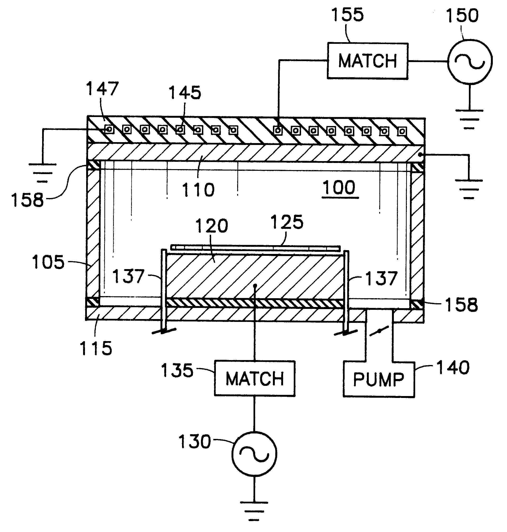
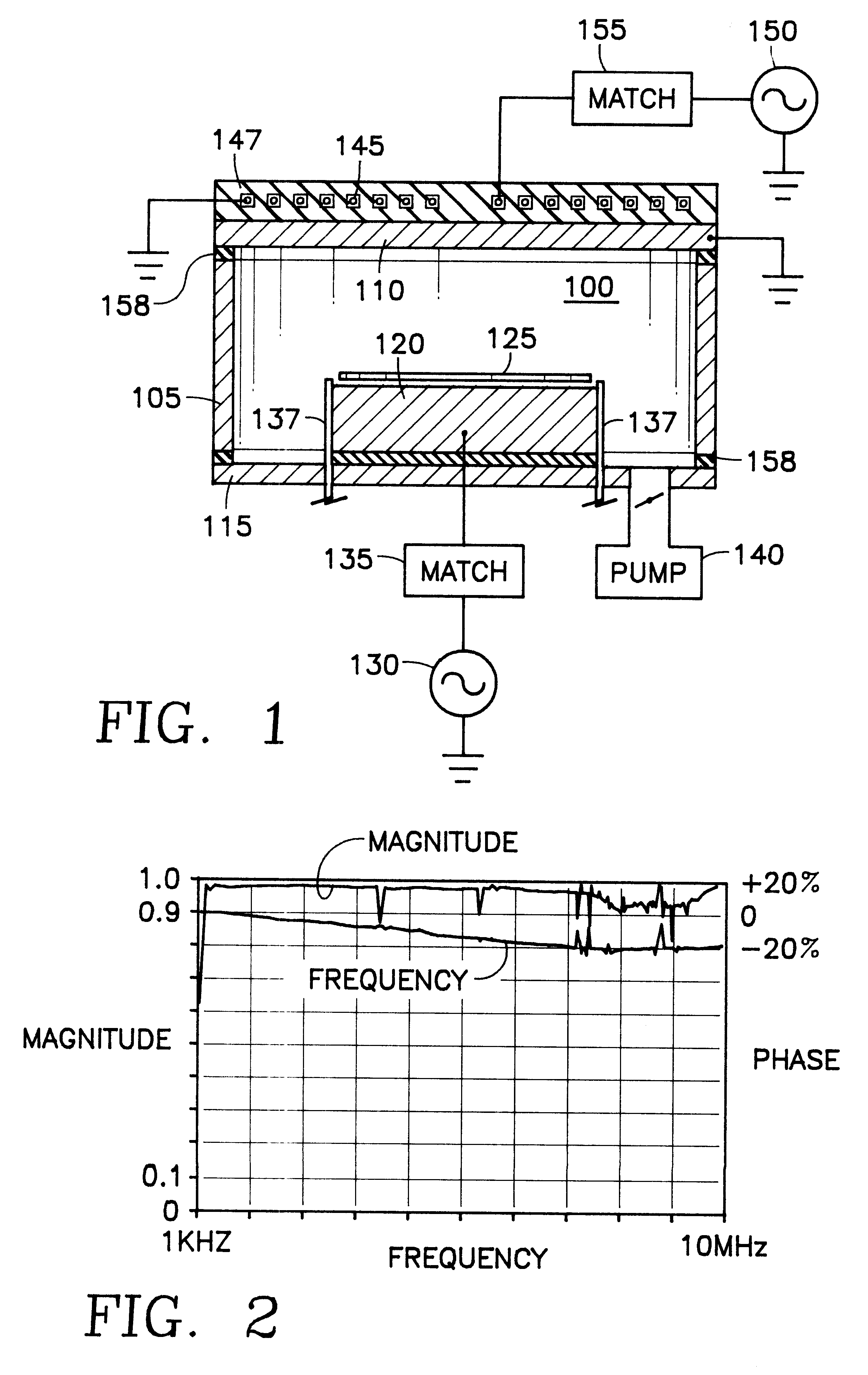
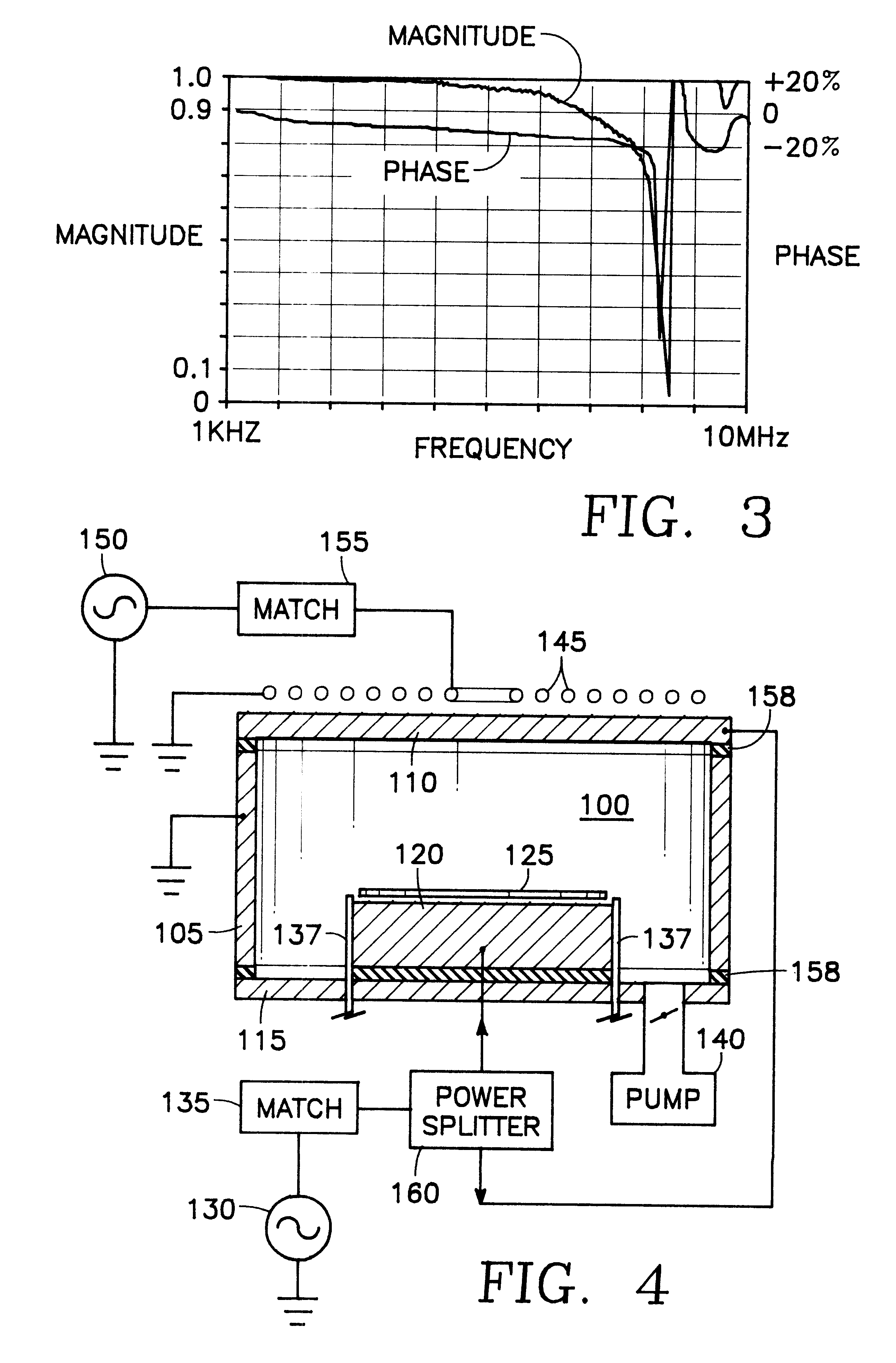
There are, however, a number of potential problems which, if not resolved, could render the reactor of FIG. 1 impractical.
First, there is the problem of whether the silicon ceiling 110 will block the RF induction field of the overhead coil antenna 145 from ever reaching the chamber 100.
Also, the RF induction field skin depth through the plasma in the chamber 100 may be greater than the chamber height (i.e., the wafer-top electrode gap), so that the RF induction power may not be efficiently coupled to the plasma.
Another problem is that the close proximity of the ceiling 110 to the wafer 125 may be insufficient to separate the plasma sheath near the ceiling 110 from the plasma sheath near the underlying wafer 125, thereby shorting out the plasma from top to bottom.
Also, insertion of the silicon material of the ceiling 110 into the RF return path of the bias RF power generator 130 may occasion significant RF bias power losses.
Finally, there may not exist a suitable or practical range of resistivity values for the semiconductor window within which an RF inductive field can be coupled without undue loss or attenuation.

Method used


Image

  • Parallel-plate electrode reactor having an inductive antenna coupling power through a parallel plate electrode
  • Parallel-plate electrode reactor having an inductive antenna coupling power through a parallel plate electrode
  • Parallel-plate electrode reactor having an inductive antenna coupling power through a parallel plate electrode

Examples


Embodiment Construction

While the silicon ceiling 110 is grounded in the preferred embodiment of FIG. 1, in the embodiment FIG. 4 power from the RF generator 130 is split by a power splitter 160 between the pedestal 120 and the silicon ceiling 110. In order to provide a ground return path, the side wall 105 may be a grounded conductor. In FIG. 5, the silicon ceiling 110 is driven independently from the wafer pedestal 120 by a separate RF power generator 165 through a conventional impedance match circuit 170. While the embodiment of FIG. 1 employs a single coil as the inductor antenna 145, in the embodiment of FIG. 6 the inductor antenna 145 is comprised of plural (in this case, two) independently driven coils, namely an inner coil 175 overlying the wafer center and an outer coil 180 overlying the wafer periphery. In the implementation of FIG. 6, the inner and outer coils 175, 180 are planar concentric coils driven by separate plasma source power generators 185, 190. The advantage is that plasma variations ...


PUM

PropertyMeasurementUnit
pressureaaaaaaaaaa
depthaaaaaaaaaa
sizesaaaaaaaaaa

Abstract

The invention is embodied by a plasma reactor for processing a workpiece, including a reactor enclosure defining a processing chamber, a semiconductor window, a base within the chamber for supporting the workpiece during processing thereof, a gas inlet system for admitting a plasma precursor gas into the chamber, and an inductive antenna adjacent a side of the semiconductor window opposite the base for coupling power into the interior of the chamber through the semiconductor window electrode.

Description

1. Technical FieldThe invention relates to a plasma reactor having parallel plates for interposition therebetween of a workpiece to be processed, such as a semiconductor wafer, and an inductive coil antenna coupling RF power through one of the parallel plates into the interior of the reactor.2. Background ArtInductively coupled plasma reactors for processing microelectronic semiconductor wafers, such as the type of reactor disclosed in U.S. Pat. No. 4,948,458 to Ogle, enjoy important advantages over parallel-plate capacitively coupled plasma reactors. For example, inductively coupled plasma reactors achieve higher plasma ion densities (e.g., on the order of 10.sup.11 ions / cm.sup.3). Moreover, plasma ion density and plasma ion energy can be independently controlled in an inductively coupled plasma reactor by applying bias power to the workpiece or wafer. In contrast, capacitively coupled reactors typically provide relatively lower plasma ion densities (e.g., on the order of only 10.s...

Claims


Application Information

Patent Timeline
Patent Type & Authority Patents(United States)
IPC IPC(8): H01J37/32H01L21/683H01L21/67
CPCH01J37/321H01J37/32165H01J37/32458H01J37/32467H01L21/6831H01J37/32871H01J37/32522H01J2237/3345H01J2237/3346
Inventor COLLINS, KENNETH S.
Owner APPLIED MATERIALS INC
Why Eureka
Try Eureka