Stacked dual-band electromagnetic band gap waveguide aperture with independent feeds

Inactive Publication Date: 2010-03-30
ROCKWELL COLLINS INC
View PDF5 Cites 10 Cited by
  • Summary
  • Abstract
  • Description
  • Claims
  • Application Information

AI Technical Summary

Benefits of technology

[0029]It is an advantage of the present invention to provide about 360° phase shift at widely spaced frequencies.
[0030]It is an advantage of the present invention to provide dual-band operation with the same polarization or orthogonal pola

Problems solved by technology

One of the major challenges in ESA design is to provide cost effective antenna array phase shifting methods and techniques along with dual-band operation of the ESA.
Smaller apertures yield greater phase shift per unit length

Method used


Image

  • Stacked dual-band electromagnetic band gap waveguide aperture with independent feeds
  • Stacked dual-band electromagnetic band gap waveguide aperture with independent feeds
  • Stacked dual-band electromagnetic band gap waveguide aperture with independent feeds

Examples


Embodiment Construction

[0051]The present invention is for a dual-band stacked electromagnetic band gap (EBG) waveguide aperture electronically scanned array (ESA) antenna with independent feeds.

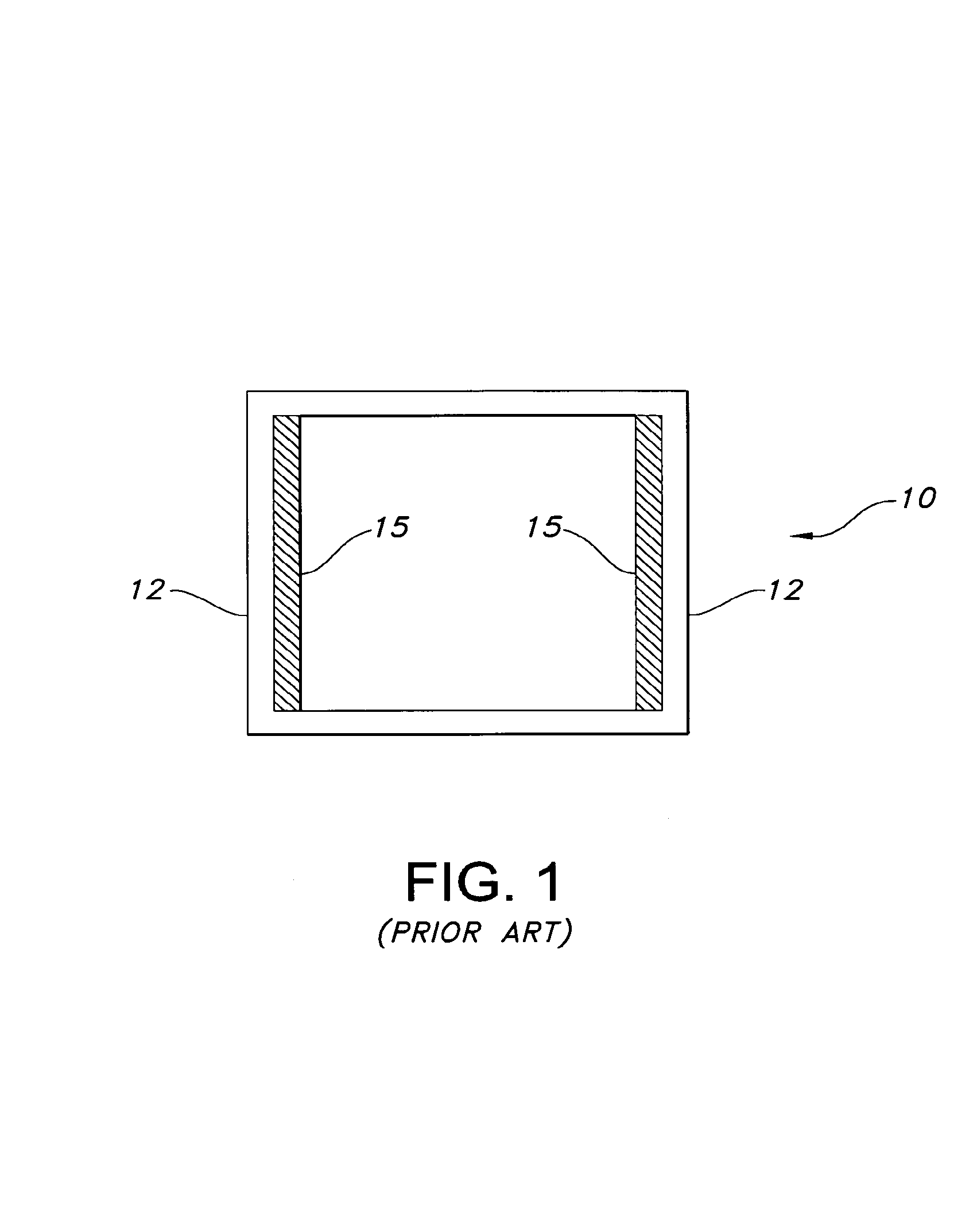
[0052]A prior art single-mode analog waveguide phase shifter 10 using electromagnetic band gap (EBG) devices 15 on waveguide sidewalls 12 is shown in FIG. 1 and is described in the referenced paper by J. A. Higgins et al. and disclosed in U.S. Pat. No. 6,756,866. The references describe electromagnetic crystal (EMXT) devices implemented with EBG materials. EBG materials are periodic dielectric materials that forbid propagation of electromagnetic waves in a certain frequency range. The EBG material may be GaAs, ferroelectric, ferromagnetic, or any suitable EBG embodiment. EMXT device and EBG device are used interchangeably in the following description.

[0053]The waveguide sidewalls 12 of the prior art single-mode EBG waveguide phase shifter 10 in FIG. 1 each contain an EBG device 15 that consists of a periodic surfac...


PUM


Abstract

A dual-band stacked electromagnetic band gap (EBG) electronically scanned array (ESA) has a high-frequency aperture stacked on a low-frequency aperture. The high-frequency aperture looks through the low-frequency aperture. Low-frequency and high-frequency feeds feed the apertures. The low-frequency aperture comprises low-frequency cells with two vertical low-frequency EBG sidewalls and two horizontal metal walls. The high-frequency aperture comprises high-frequency cells with four cells stacked on each of the low-frequency cells. The four high-frequency cells comprise four vertical high-frequency EBG sidewalls, two horizontal metal top and bottom metal walls, and a center horizontal metal wall for operation with the same polarization as the low-frequency aperture. The high-frequency cells may comprise four horizontal high-frequency EBG sidewalls, two vertical left and right metal walls, and a center vertical metal wall for orthogonal polarization. A frequency selective surface may be used to provide isolation between the apertures.

Description

CROSS REFERENCE TO RELATED APPLICATIONS AND PATENTS[0001]The present application is related to co-filed application Ser. No. 11 / 495,381 entitled “Stacked Dual-Band Electromagnetic Band Gap Waveguide Aperture for an Electronically Scanned Array” by Brian J. Herting. The present application is related to application Ser. No. 11 / 154,256 filed on Jun. 16, 2005 entitled “Low-Loss, Dual-Band Electromagnetic Band Gap Electronically Scanned Antenna Utilizing Frequency Selective Surfaces” by Brian J. Herting, now issued as U.S. Pat. No. 7,151,508. The present application is related to U.S. Pat. No. 6,822,617 entitled “A Construction Approach for an EMXT-Based Phased Array Antenna” by John C. Mather, Christina M. Conway, James B. West, Gary E. Lehtola, and Joel M. Wichgers; and U.S. Pat. No. 6,950,062 entitled “A Method and Structure for Phased Array Antenna Interconnect” by John C. Mather, Christina M. Conway, and James B. West. The patents and applications are incorporated by reference here...

Claims


Application Information

Patent Timeline
IPC IPC(8): H01Q3/36H01P5/12
CPCH01P1/182H01P1/2005H01Q5/47H01Q5/42H01Q21/064H01Q5/0075H01Q5/0082
Inventor WEST, JAMES B.
Owner ROCKWELL COLLINS INC
Why Eureka
Try Eureka