
Power amplifying device having linearizer

a technology of power amplifying device and linearizer, which is applied in the direction of amplifiers, amplifiers with semiconductor devices only, amplifiers with semiconductor devices, etc., can solve the problems of signal distortion components, degrade the transmission performance of the telecommunication system, and not having the maximum output region having maximum efficiency, so as to improve the linearity of output signals.

Inactive Publication Date: 2010-04-06
SAMSUNG ELECTRO MECHANICS CO LTD
View PDF6 Cites 10 Cited by
  • Summary
  • Abstract
  • Description
  • Claims
  • Application Information

AI Technical Summary

Benefits of technology

[0016]An aspect of the present invention provides a power amplifying device, and more particularly, to a power amplifying device having a linearizer, in which a bias circuit has an initial impedance set when initially operated, then the impedance is varied according to a level of an input signal and the input signal is amplified in a broad range from a low level region to a high level region, thereby improving linearity of an output signal.

Problems solved by technology

In general, a power amplifying device essentially employed in a wireless telecommunication system, when operating in a saturation region having nonlinear characteristics, experiences distortion in size and phase of an output signal due to the nonlinear characteristics, thereby generating signal distortion components.
In consequence, this significantly degrades transmission performance of the telecommunication system.
However, in this back-off method, the power amplifying device is operated in a several dB low region, which is not a maximum output region having maximum efficiency.
This as a result considerably undermines efficiency of the power amplifying device.
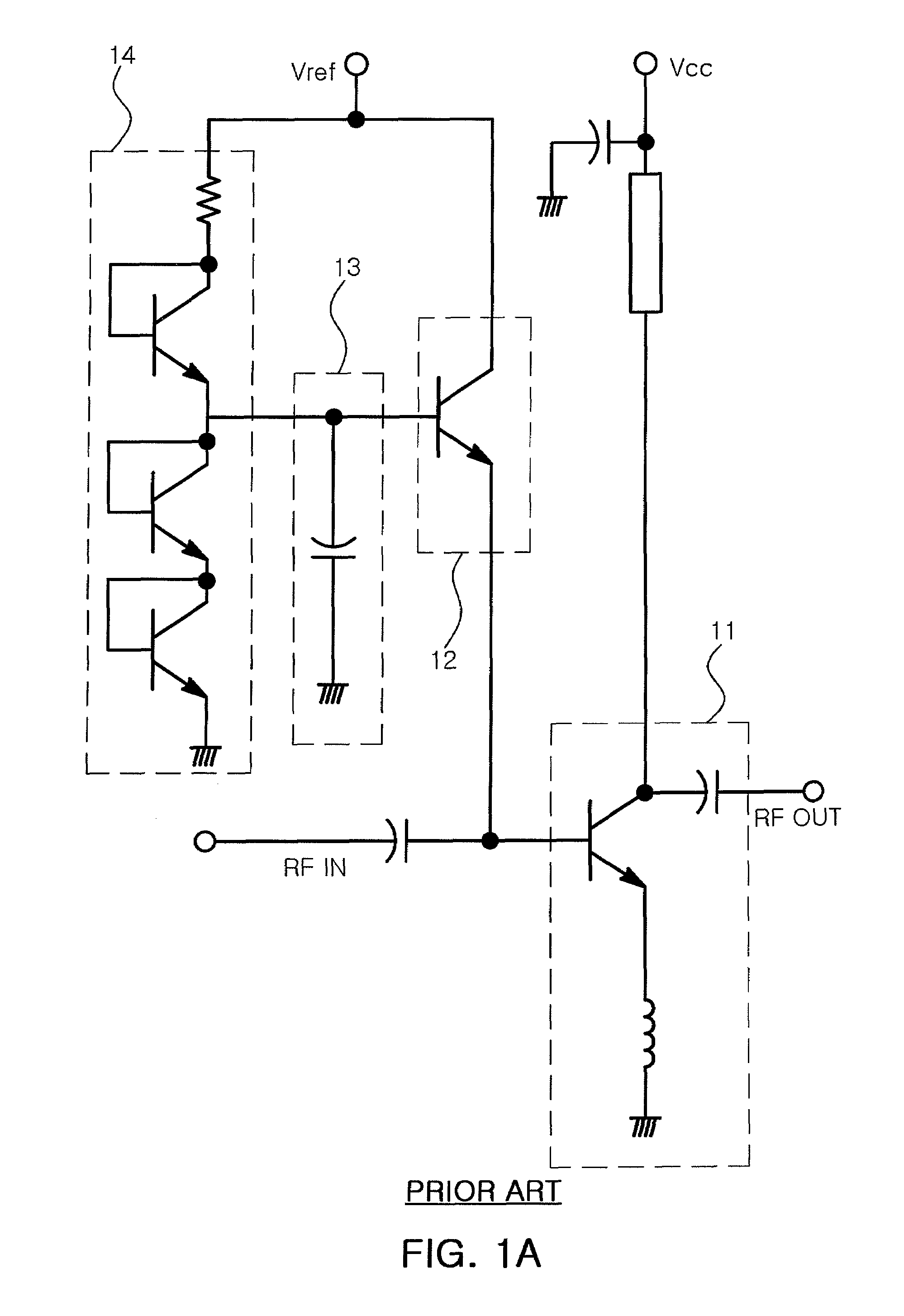
Thus, in a case where the input signal RF IN has a low level, the fixed capacitance leads to a low impedance, thereby increasing current consumption and degrading efficiency.

Method used


Image

  • Power amplifying device having linearizer
  • Power amplifying device having linearizer
  • Power amplifying device having linearizer

Examples


Embodiment Construction

[0036]Exemplary embodiments of the present invention will now be described in detail with reference to the accompanying drawings.

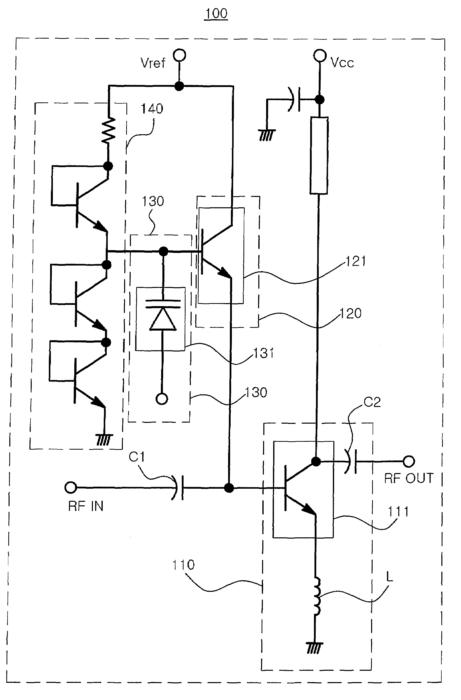
[0037]FIG. 2 is a circuit diagram illustrating a power amplifying device according to an exemplary embodiment of the invention.

[0038]Referring to FIG. 2, the power amplifying device 100 of the present embodiment includes an amplifying unit 110, a bias unit 120, an impedance setting unit 130 and a current compensating unit 140.

[0039]The amplifying unit 110 includes at least one amplifying transistor 111, and the amplifying transistor 111 includes a base receiving an input signal RF IN, a collector receiving an operating power source Vcc and an emitter connected to a ground. A coupling capacitor C1 is connected in series between the base and an input signal RF IN terminal. Also, another coupling capacitor C2 is connected in series between the collector and an output signal RF OUT terminal. An inductor L is connected in series between the ground and the emitt...


PUM


Abstract

There is provided a power amplifying device having a linearizer in which a bias circuit has an initial impedance set when initially operated, then the impedance is varied according to a level of an input signal and the input signal is amplified in a broad range from a low level region to a high level region, thereby improving linearity of an output signal. The power amplifying device including: an amplifying unit receiving a bias power source and amplifying an input signal; a bias unit varying the bias power source according to a set impedance to provide to the amplifying unit; and an impedance setting unit setting the impedance of the bias unit in response to a preset control voltage when the bias unit is initially operated and re-setting the impedance of the bias unit according to a level of the input signal of the amplifying unit after initial operation of the bias unit.

Description

CROSS-REFERENCE TO RELATED APPLICATIONS[0001]This application claims the priority of Korean Patent Application No. 2007-30877 filed on Mar. 29, 2007, in the Korean Intellectual Property Office, the disclosure of which is incorporated herein by reference.BACKGROUND OF THE INVENTION[0002]1. Field of the Invention[0003]The present invention relates to a power amplifying device, and more particularly, to a power amplifying device having a linearizer, in which a bias circuit has an initial impedance set when initially operated, then the impedance is varied according to a level of an input signal and the input signal is amplified in a broad range from a low level region to a high level region, thereby improving linearity of an output signal.[0004]2. Description of the Related Art[0005]In general, a power amplifying device essentially employed in a wireless telecommunication system, when operating in a saturation region having nonlinear characteristics, experiences distortion in size and p...

Claims


Application Information

Patent Timeline
Patent Type & Authority Patents(United States)
IPC IPC(8): H03F3/04
CPCH03F1/0266H03F1/32H03F2200/18H03F3/20
Inventor CHO, YUN HEEPARK, CHUL SOONKIM, JI HOONPARK, YUN HWI
Owner SAMSUNG ELECTRO MECHANICS CO LTD
Learn More