Cluster tool substrate throughput optimization

a cluster tool and substrate technology, applied in the field of integrated processing system, can solve the problems of limiting the throughput of the processing sequence, limiting the robots in the track lithography process sequence, cluster tool users and manufacturers spending a large amount of tim

Active Publication Date: 2010-04-20
SCREEN SEMICON SOLUTIONS CO LTD
View PDF565 Cites 47 Cited by
  • Summary
  • Abstract
  • Description
  • Claims
  • Application Information

AI Technical Summary

Problems solved by technology

In an effort to reduce CoO, electronic device manufacturers often spend a large amount of time trying to optimize the process sequence and chamber processing time to achieve the greatest substrate throughput possible given the cluster tool architecture limitations and the chamber processing times.
The longest process recipe step will generally limit the throughput of the processing sequence.
This is usually not the case in track lithography process sequences, due to the short processing times and large number of processing steps.
A track lithography process sequences is generally robot limited due to the short processing times and large number of processing steps.
These factors are very important to a cluster tool's profitability and / or usefulness, since the longer the system is unable to process substrates the more money is lost by the user due to the lost opportunity to process substrates in the cluster tool.
Therefore, cluster tool users and manufacturers spend a large amount of time trying to develop reliable processes, reliable hardware and reliable systems that have increased uptime.
The push in the industry to shrink the size of semiconductor devices to improve device processing speed and reduce the generation of heat by the device, has caused the industry's tolerance to process variability to diminish.
Due to the shrinking size of semiconductor devices and the ever increasing device performance requirements, the allowable variability of the device fabrication process uniformity and repeatability has greatly decreased.
Lithography type device fabrication processes can be especially sensitive to variations in process recipe variables and the timing between the recipe steps, which directly affects process variability and ultimately device performance.

Method used


Image

  • Cluster tool substrate throughput optimization
  • Cluster tool substrate throughput optimization
  • Cluster tool substrate throughput optimization

Examples


Embodiment Construction

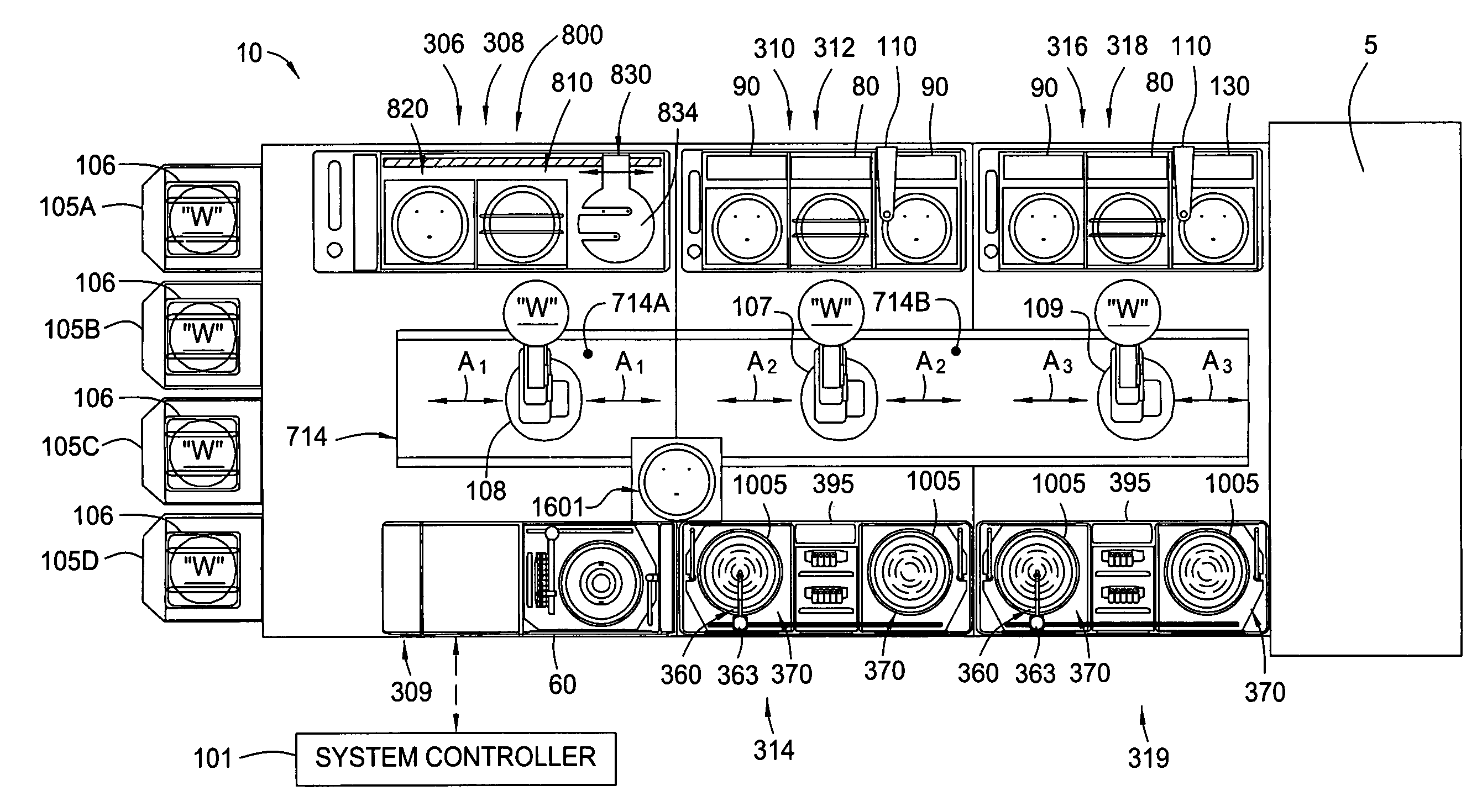
[0054]The present invention generally provides an apparatus and method for processing substrates using a multi-chamber processing system (e.g., a cluster tool) that has an increased system throughput, increased system reliability, and a more repeatable wafer processing history (or wafer history) within the cluster tool. In one embodiment, the cluster tool is adapted to perform a track lithography process in which a substrate is coated with a photosensitive material, is then transferred to a stepper / scanner, which exposes the photosensitive material to some form of radiation to form a pattern in the photosensitive material, and then certain portions of the photosensitive material are removed in a developing process completed in the cluster tool.

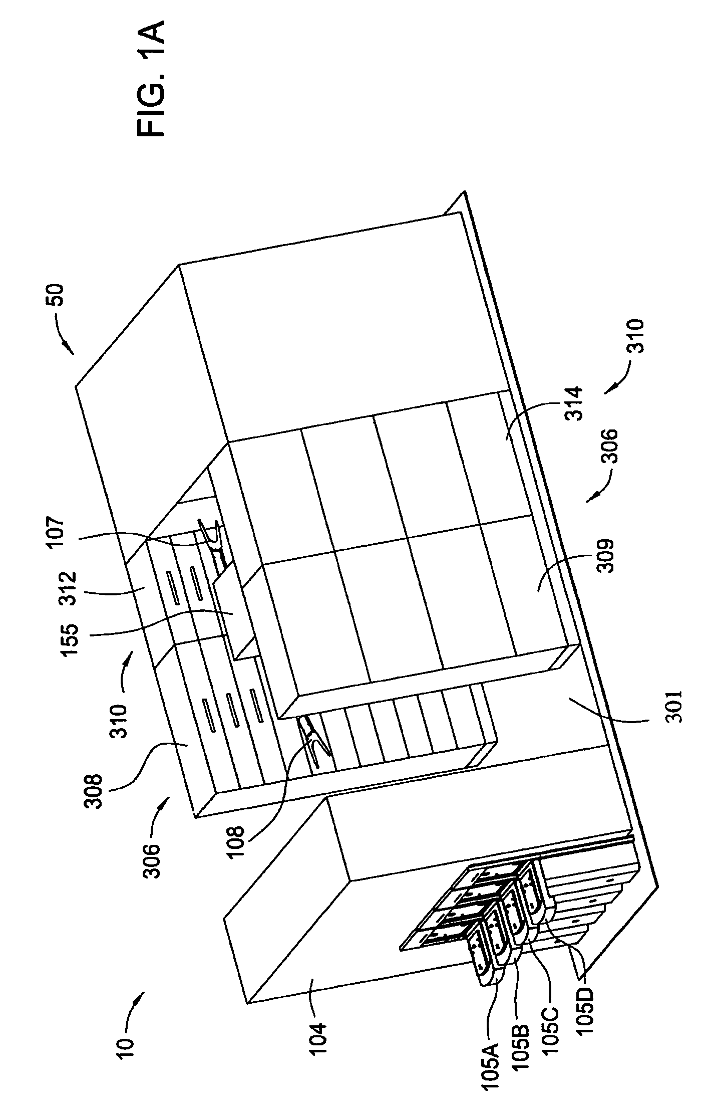
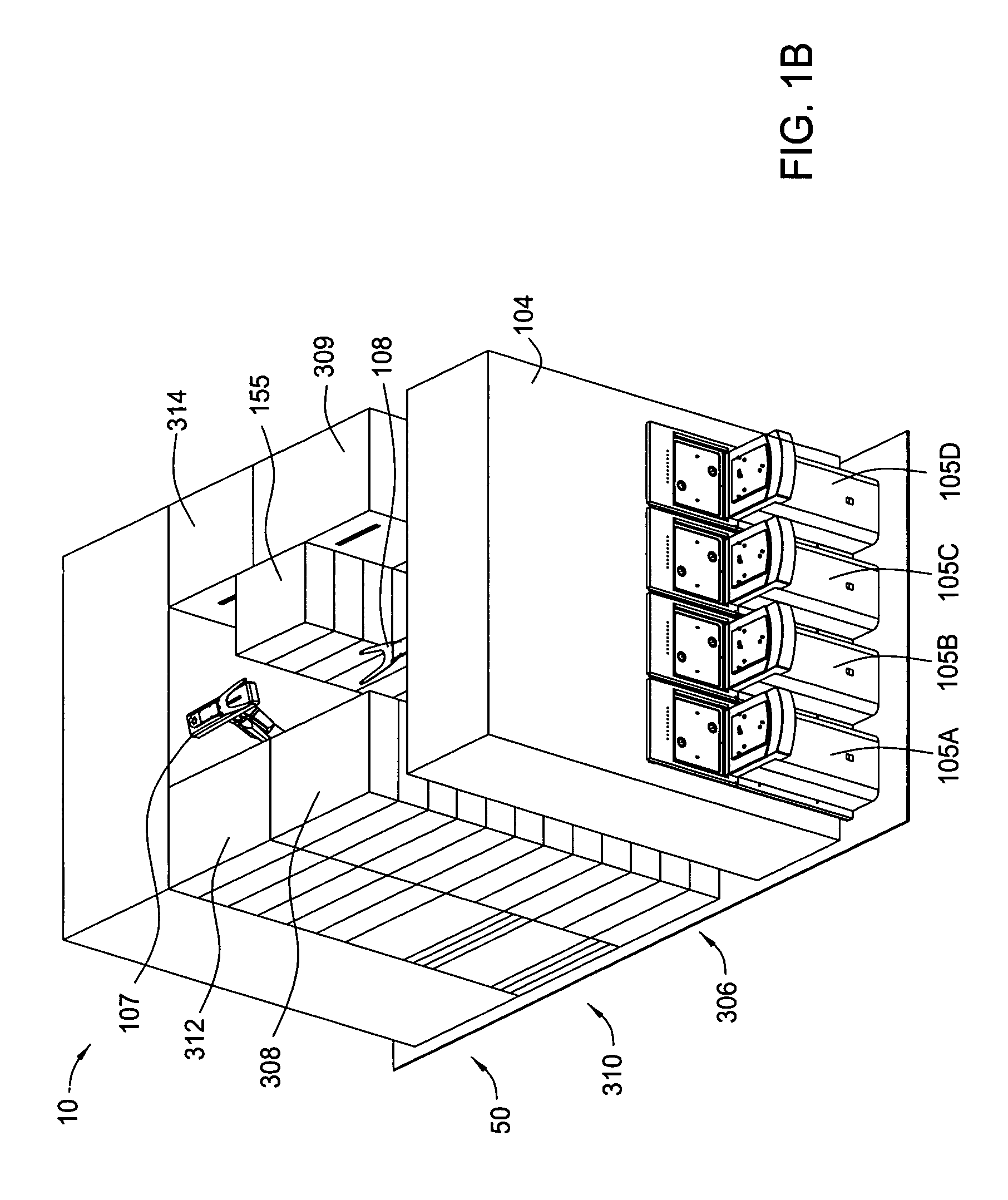
[0055]FIGS. 1A and 1B are isometric views of one embodiment of a cluster tool 10 that illustrates a number of the aspects of the present invention that may be used to advantage. One embodiment of the cluster tool 10, as illustrated in FIGS. 1A...


PUM

PropertyMeasurementUnit
temperatureaaaaaaaaaa
distanceaaaaaaaaaa
distanceaaaaaaaaaa

Abstract

Embodiments generally provide an apparatus and method for processing substrates using a multi-chamber processing system (e.g., a cluster tool) that has an increased system throughput, increased system reliability, substrates processed in the cluster tool have a more repeatable wafer history. In one embodiment, non-orthogonal robot trajectories are used to assure reliable and high speed substrate transfer. In another embodiment, at least one buffering station is used to avoid collision and improve throughput. In another embodiment, optimal positioning of the robots are used to improve throughput.

Description

CROSS-REFERENCE TO RELATED APPLICATIONS[0001]This application is a continuation-in-part of U.S. patent application Ser. No. 11 / 112,281, filed Apr. 22, 2005, now U.S. Pat. No. 7,357,842 which claims the benefit of U.S. Provisional Patent Application Ser. No. 60 / 639,109, filed Dec. 22, 2004. Each of the aforementioned related patent applications is herein incorporated by reference.BACKGROUND OF THE INVENTION[0002]1. Field of the Invention[0003]Embodiments of the invention generally relate to an integrated processing system containing multiple processing stations and robots that are capable of processing multiple substrates in parallel.[0004]2. Description of the Related Art[0005]The process of forming electronic devices is commonly done in a multi-chamber processing system (e.g., a cluster tool) that has the capability to sequentially process substrates, (e.g., semiconductor wafers) in a controlled processing environment. A typical cluster tool used to deposit and develop a photoresis...

Claims


Application Information

Patent Timeline
Patent Type & Authority Patents(United States)
IPC IPC(8): B05C13/02C23C14/00H01L21/677
CPCG03B27/32H01L22/26G03F7/40H01L21/67109H01L21/6715H01L21/67161H01L21/67173H01L21/67178H01L21/67184H01L21/6719H01L21/67225H01L21/67742H01L21/67745H01L21/67748H01L21/6831H01L21/6838G03D13/006Y10S414/136Y10S414/135
Inventor VOLFOVSKI, LEONISHIKAWA, TETSUYA
Owner SCREEN SEMICON SOLUTIONS CO LTD
Why Eureka
Try Eureka