Semiconductor memory device

a memory device and semiconductor technology, applied in the field of semiconductor memory devices, can solve the problems of increasing the resistance of the bit line in the lower layer, reducing the operation speed of the dram, and reducing so as to shorten the local bit line length, reduce the resistance of the bit line, and high-density memory cell array

Inactive Publication Date: 2010-04-20
LONGITUDE SEMICON S A R L
View PDF9 Cites 14 Cited by
  • Summary
  • Abstract
  • Description
  • Claims
  • Application Information

AI Technical Summary

Benefits of technology

[0008]An object of the present invention is to provide a semiconductor memory device in which a hierarchical memory cell array is configured, memory cells connected to a local bit line can be highly integrated so as to suppress an increase in chip area, and a decrease in operation speed caused by an increase in a bit line resistance can be effectively prevented when employing a vertical type transistor and an embedded bit line structure.
[0010]According to the semiconductor memory device of the present invention, in a hierarchical memory cell array, the local bit lines partitioned into N sections along the global bit line are arranged, a signal read out from a memory cell formed at an intersection of a word line and a local bit line is amplified by the local sense amplifier through the local bit line, and the signal is further transmitted to the global bit line so as to be coupled to the external data line. Thus, even when low resistance material cannot be used for forming the local bit line due to structural restriction in order to connect the local bit line arranged below the memory cell using a vertical transistor structure, it is possible to suppress the overall bit line resistance by shortening the length of the local bit line. Thereby, a decrease in operation speed caused by an increase in the bit line resistance can be effectively prevented, and an increase in chip area can be suppressed by arranging memory cells with higher density.
[0016]As described above, according to the present invention, by employing a hierarchical memory cell array, the entire semiconductor memory device is configured by arranging local bit lines partitioned into N sections along the global bit line, and the vertical transistor structure connected to a lower local bit line is employed in each memory cell to achieve a high-density memory cell array. Thereby, even if the local bit line cannot be formed using low resistance material due to a structural restriction, the bit line resistance can be reduced by shortening the length of the local bit line and a decrease in operation speed can be prevented when reading a signal. Further, memory cells having a small size as 4F2 can be achieved using the structure of memory cells and the simple single-ended local sense amplifiers, and thus an increase in the entire chip area can be suppressed.

Problems solved by technology

However, if the embedded bit line structure is employed, it is difficult to form a bit line arranged in a lower layer using metal or silicide having a low resistance.
Therefore, the bit line needs to be formed using polysilicon or a diffusion layer, which inevitably causes the resistance thereof to increase, and it arises a problem of a decrease in operation speed of the DRAM.
Thereby, a bit line resistance can be suppressed, but a complex structure is required for withdrawing the bit line upward, and it is undesirable in terms of an increase in the number of manufacturing steps and an increase in cost.
However, the bit line resistance becomes larger than that in a case of using the metal or silicide, and it is a problem that the operation speed further decreases.
In this manner, when the memory cell array is configured by employing the vertical type transistor and the embedded bit line structure, it is difficult to prevent a decrease in the operation speed caused by an increase in the bit line resistance without deterioration of manufacturing and cost.

Method used


Image

  • Semiconductor memory device
  • Semiconductor memory device
  • Semiconductor memory device

Examples


first embodiment

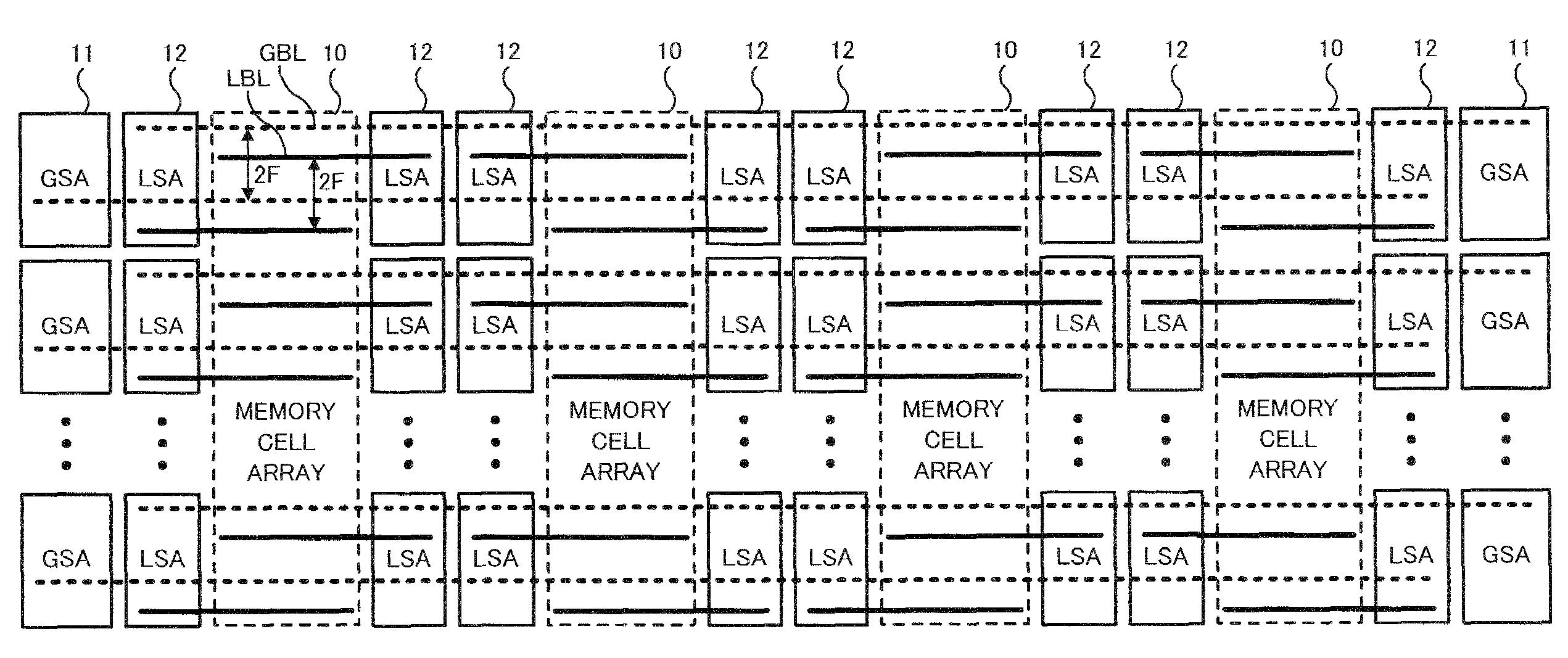
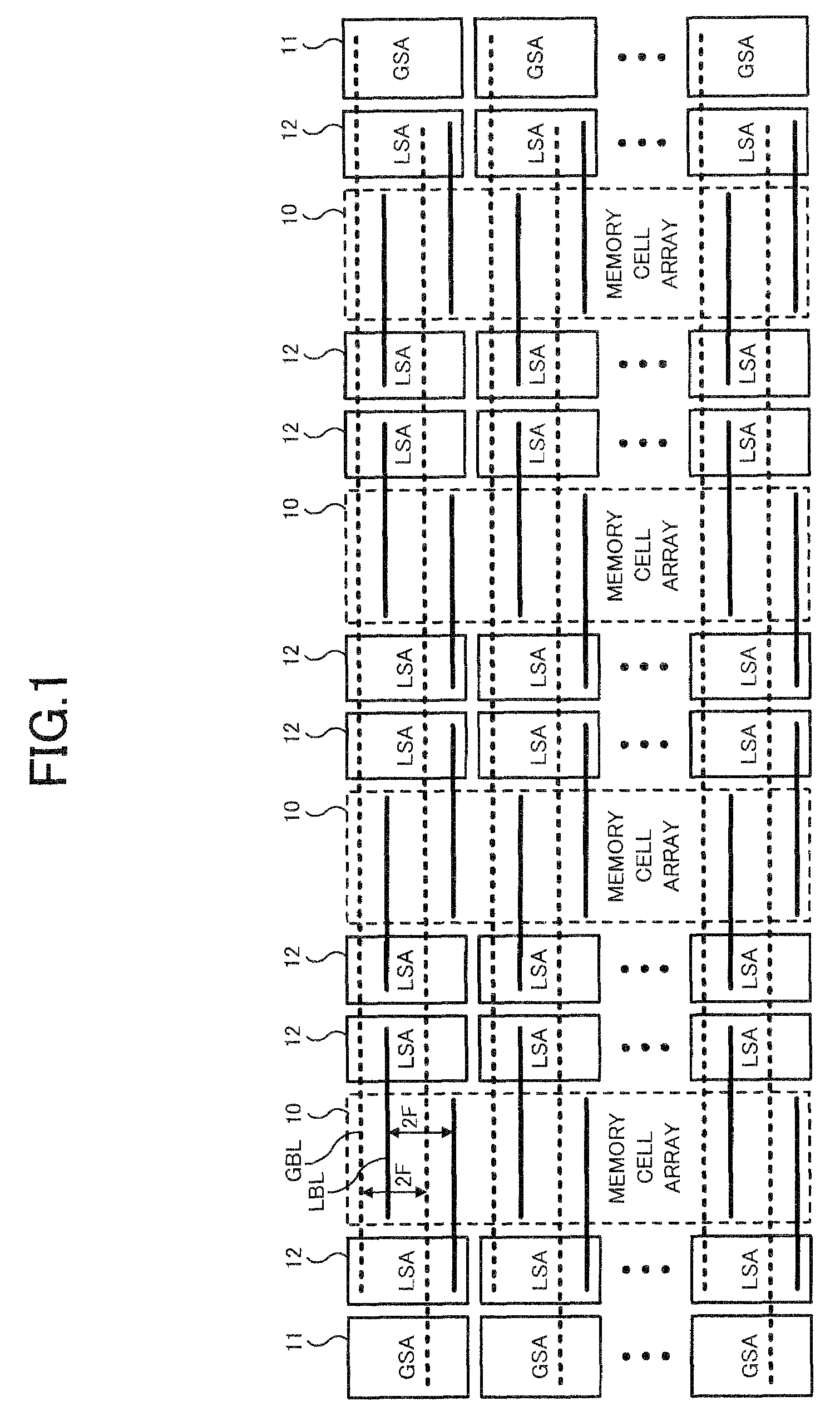
[0030]A first embodiment of the present invention will be described first. FIG. 1 shows an entire configuration of the DRAM of the first embodiment. In FIG. 1, there are shown four memory cell arrays 10, a plurality of global sense amplifiers 11, a plurality of local sense amplifiers 12, a plurality of global bit lines GBL, and a plurality of local bit lines LBL.

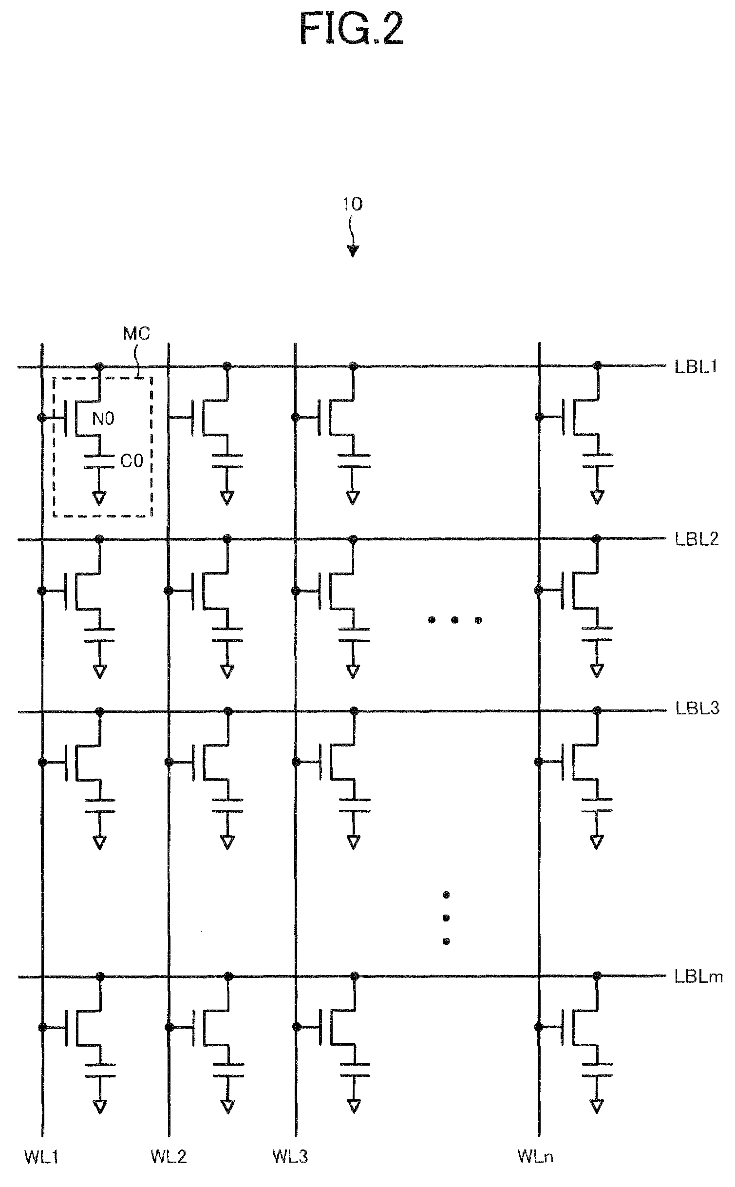
[0031]Each memory cell array 10 includes a large number of memory cells formed at all intersections of a plurality of word lines and the plurality of local bit lines LBL intersecting therewith. As shown in FIG. 1, the plurality of local bit lines LBL is regularly aligned with a pitch 2F based on a design rule value F in a word line extending direction. Besides, the plurality of global bit lines GBL is also aligned with the same pitch 2F as the local bit lines LBL.

[0032]The local sense amplifiers 12 are arranged on both sides of the memory cell arrays 10, and each local sense amplifier 12 amplifies a signal read from a memory...

second embodiment

[0060]A second embodiment of the present invention will be described. The DRAM of the second embodiment differs from the entire configuration of DRAM of the first embodiment in that adjacent memory cell arrays 10 share a local sense amplifier 20. FIG. 8 shows an entire configuration of the DRAM of the second embodiment. In FIG. 8, there are shown four memory cell arrays 10, a plurality of global sense amplifiers 11, a plurality of shared local sense amplifiers 20, a plurality of non-shared local sense amplifiers 21, a plurality of global bit lines GBL, and a plurality of local bit lines LBL.

[0061]In FIG. 8, configurations of the four memory cell arrays 10 and the plurality of global sense amplifiers 11 are common to those of FIG. 1. Meanwhile, in an area including two adjacent global bit lines GBL, three shared local sense amplifiers 20 are arranged between memory cell arrays 10, and two non-shared local sense amplifiers 21 are arranged at both ends of the four memory cell arrays 10...


PUM


Abstract

A semiconductor memory device comprises: word lines; global bit lines intersecting therewith; local bit lines partitioned into N sections along the global bit lines and aligned with a same pitch as the global bit lines; N memory cell arrays each of which includes memory cells each having a vertical transistor structure connected to the local bit lines at a lower portion and each being formed at an intersection of the word line and the local bit line, and is arranged corresponding to each section of the local bit lines; local sense amplifiers for amplifying a signal read out from a selected memory cell to the local bit line and for outputting the signal to the global bit line; and global sense amplifiers for coupling the signal transmitted from the local sense amplifier corresponding to the selected memory cell through the global bit line to an external data line.

Description

BACKGROUND OF THE INVENTION[0001]1. Field of the Invention[0002]The present invention relates to a semiconductor memory device which rewritably stores data in a plurality of memory cells formed at intersections of a plurality of word lines and a plurality of bit lines, and particularly relates to a semiconductor memory device employing an embedded bit line structure which is located below a vertical type transistor formed in each memory cell.[0003]2. Description of the Related Art[0004]Generally, a memory cell array of a DRAM includes a large number of memory cells formed at intersections of bit lines and word lines. In recent years, attention is paid to a technique using a vertical type transistor as a memory cell structure of the DRAM (e.g., see Patent References 1 and 2). In order to form a fine memory cell with a design rule such as 4F2, it is advantageous for integration and manufacturing to configure the memory cell array using vertical type transistors. On the premise of the ...

Claims


Application Information

Patent Timeline
Patent Type & Authority Patents(United States)
IPC IPC(8): G11C7/02
CPCG11C11/4097
Inventor KAJIGAYA, KAZUHIKO
Owner LONGITUDE SEMICON S A R L
Why Eureka
Try Eureka